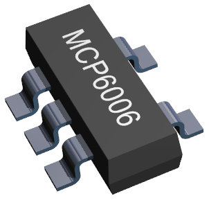
A Typical Part
What is a part? That is a good question. For AutoTRAX DEX, a part can be one of several different things. These are physical parts, which can either be electrical or purely mechanical and non-physical parts which can also be electrical but can also be meta data such as sheet title blocks or just graphics.
Physical Parts
The first, and most obvious type is a physical part.
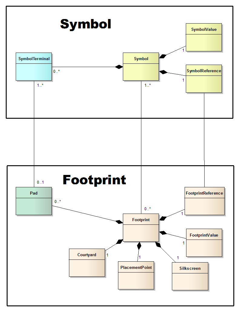
In AutoTRAX DEX, a physical part as many different representations. These are symbolic shapes, physical land patterns and 3-D physical models
The first representation is a logical or symbolic form. This is where the part is represented by a graphical symbol.
The second representation is as a 2-D footprint or land pattern. This 2-D representation is a collection of objects which include pads, silkscreen artwork, reference IDs, placement points, PCB holes, PCB cutouts and even the PCB shape or outline.
The third and final representation is a 3-D model that shows you are way part actually exist in reality. This is the closest of the three representations that matches what a physical part really looks like.
Most parts consist of:
•1 or more symbols
•1 footprint
•1 3D model
•An optional Spice simulation model.
Symbols
A part can consist of one or more symbols. Each symbol represents the electrical characteristics of the part and also is the main visualization of the part.
There are 2 types of symbols. Terminal Magnet based symbols and custom symbols.
Terminal Magnet based symbols
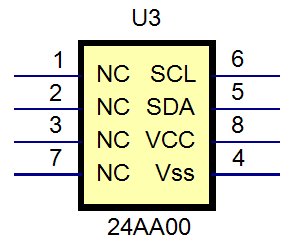
A symbol using a terminal magnet
Custom Symbols
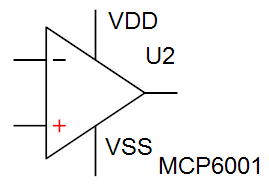
A symbol not using terminal magnet
Single Symbol
Most parts consist of a single symbol.
Multiple Symbols
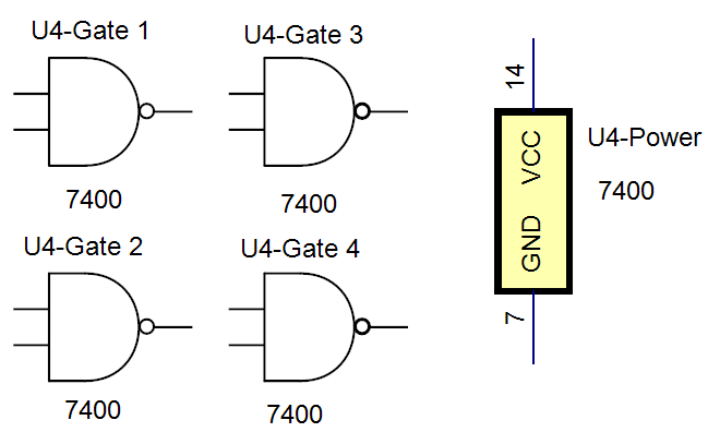
A part can have more than one symbol. Here you have a symbol that has been represented by 4 different logical get symbols and one power connection symbol using a terminal magnet.
Or you can split a symbol as many different symbols as you wish. For instance below the single symbol on the left has been split into five separate symbols whether functionality has been grouped into each symbol. This makes the understanding of the design a lot easier. You can split a symbol into multiple symbols at you have placed a symbol onto a schematic sheet.
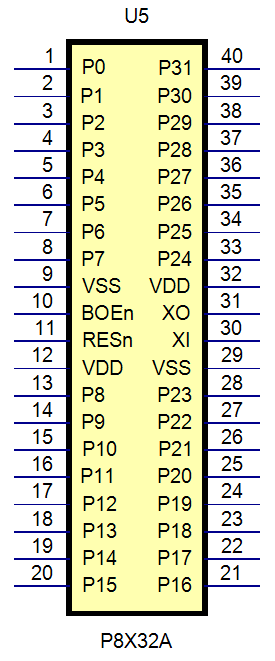
The single symbol
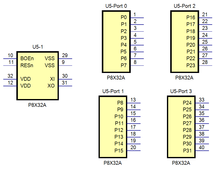
The above symbol split into five separate symbols to clearly reflect the functionality of the device
Footprints or Land-Patterns
A footprint is literally the footprint of a part on the PCB. The most obvious part of the footprint is the collection of electrical contact pads the electrically connect the electrical terminals of a part to copper tracks which also connect to contact pads belonging to the footprints of other parts.
In addition the contact pads act as 'glue' point to stick the parts to the PCB. The 'glue' is not an organic based adhesive but instead is an alloy (solder) that melts at just above 200°C and bonds to the copper pads and the leads of the part.
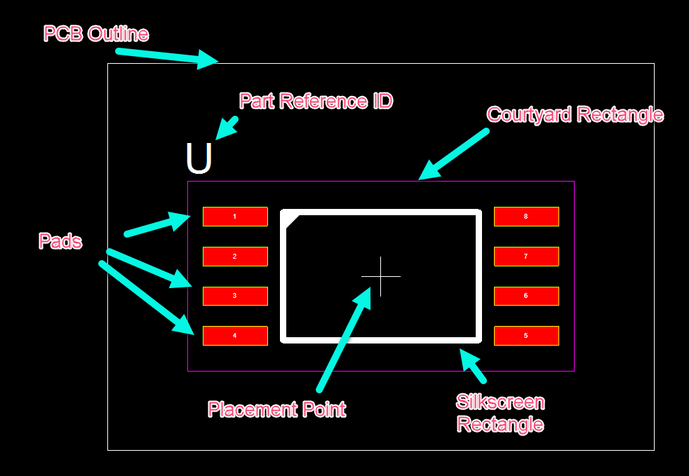
In addition to the contact pads (pads) the footprint also have:
•A Silkscreen Pattern
•A Courtyard rectangle
The 3D Model
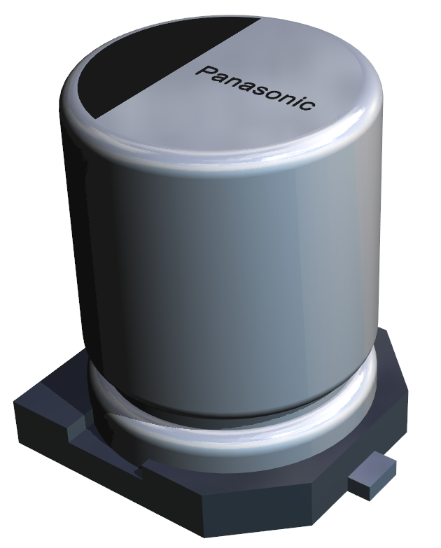 Each part usually has an associated 3D model to represent the part in the 3D view of the PCB. Parametric parts generate the 3D model automatically saving you a great deal of time - 3D models are difficult and time consuming to make. On the right is a 3D model for a capacitor that has been automatically created from the parameters defining the parts.
3D models can be very large in memory size and can greatly increase the size of your part and project files by several megabytes for each part. The beauty of parametric parts is that the model is generated 'on the fly' when needed from the parameters of the parts. This greatly reduces the storage required from several megabytes to just 10's of bytes.
It is also possible to import a 3D model either created by yourself or somebody in your team or imported from the Internet.