Silkscreens or artworks that are printed on the top and/or bottom of the PCB. The unknown electrical significance and are only for human consumption, mainly for use during manual assembly and for field service engineers. For cost sensitive PCBs the silkscreen will usually be omitted to say money.
Also a side-effect of silk screens when they are used to define part reference IDs is that the consume PCB area and can cause problems when you're trying to design a compact PCB.
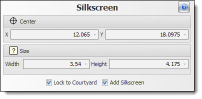
In PCB design, the term "silkscreen" refers to the layer(s) of ink markings added to the board's surface to indicate information about component placement, orientation, and other pertinent details. When referring to a component's "footprint silkscreen," it means the specific silkscreen elements associated with that particular component.
Here are some of the typical elements and considerations for footprint silkscreens:
•Component Identifier (Reference Designator):
•This is perhaps the most crucial element. It's a unique label like "R1" for the first resistor, "C2" for the second capacitor, and so on. It helps technicians and engineers locate and identify components on the board.
•Component Outline:
•Many footprints will include a rough outline of the component, showing its size and shape. This provides a visual guide during manual assembly or inspection.
•Pin 1 Indicator:
•Especially important for ICs and connectors, this marker (often a dot, triangle, or notch) indicates the position of the first pin to ensure proper component orientation during assembly.
•Polarity Indicators:
•For components like diodes, electrolytic capacitors, or polarized connectors, the silkscreen might indicate the positive (+) or negative (-) terminal.
•Component Value:
•Sometimes, especially for prototypes or boards not intended for commercial production, the value or rating of a component might be printed on the silkscreen (e.g., "10k" for a 10-kilohm resistor).
•Logos or Branding:
•Some PCBs may include company logos, certification marks, or other branding elements in the silkscreen layer.
•Scan Codes or QR Codes:
•For advanced manufacturing or tracking purposes, QR codes or other scannable elements might be added to the silkscreen.
•Considerations and Best Practices:
•Legibility: Ensure that the silkscreen text is large enough to read. There are minimum recommended sizes, typically around 1mm in height for alphanumeric characters, but this can vary based on the manufacturer.
•Avoid Overlap: Silkscreen elements should not overlap solder pads, as this can interfere with the soldering process. It's also wise to avoid overlap with via holes or other board features.
•Spacing: Keeping a small gap between the silkscreen and the component's pads or other features can reduce the risk of manufacturing issues.
•Contrast: Ensure that the silkscreen color contrasts with the PCB solder mask color for visibility. White on green or black is common, but many color combinations are available.
•Check with Manufacturer: Always check the capabilities and recommendations of your PCB manufacturer, as they can have specific guidelines or limitations regarding silkscreen details.
The silkscreen is vital not only for assembly but also for subsequent testing, troubleshooting, and repair of the PCB. Properly designed footprint silkscreens can greatly ease these processes, ensuring a more efficient and error-free work-flow.