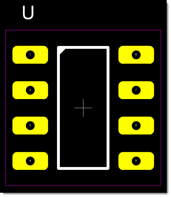
A PCB footprint, also sometimes referred to as a land pattern, is the arrangement of pads (or through-holes) on a PCB used to physically mount and electrically connect electronic components. Each type of electronic component has its unique footprint based on its physical size, type of package, and pin arrangement.

PCB Footprint

A Footprint

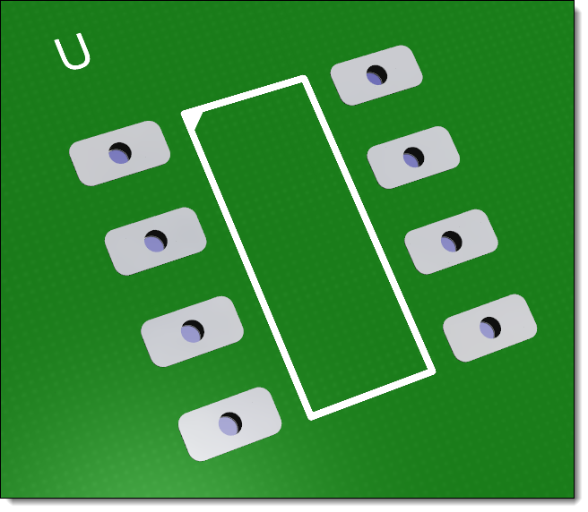
Footprint in 3D

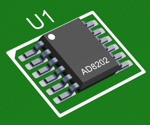
The Part for the Footprint
Here's a detailed breakdown of what PCB footprints entail:
•Pads and Through-Holes: The most basic components of footprints are the pads and through-holes. Pads are the flat surfaces on a PCB where the component leads or pins are soldered. Through-holes are the holes drilled through the PCB where through-hole components are inserted and soldered.
•Component Outline: Many footprints also include a silkscreen outline of the component to show its physical size and shape. This is beneficial during manual assembly to ensure that components are placed correctly.
•Pin Numbering: It's common for footprints to include pin numbers. This is particularly important for components with many pins or when pin orientation is crucial.
•Polarity and Orientation: For components that need to be oriented a certain way (like diodes, electrolytic capacitors, and ICs), footprints often incorporate indicators. These can be a dot, a beveled edge, or an asymmetry in the footprint design to indicate the correct orientation.
•Thermal Pads: Some components, especially high-power ones, require additional pads connected to a larger area of copper (called a thermal pad) for heat dissipation.
•Solder Paste Stencils: For surface mount devices (SMD) soldered using reflow soldering, footprints might also define areas for solder paste application.
•Special Considerations: Some components might have specific requirements. For example, RF (Radio Frequency) components might need a certain type of footprint to function correctly, or certain ICs might need a specific pattern of vias beneath them for heat dissipation.
When designing a PCB, engineers or designers will often need to create or modify footprints to match the components they are using. This ensures that the components fit properly on the PCB and that they can be soldered securely in place. Incorrect footprints can lead to assembly issues, malfunctioning circuits, or reduced reliability. Therefore, accuracy and attention to detail in footprint creation are crucial.
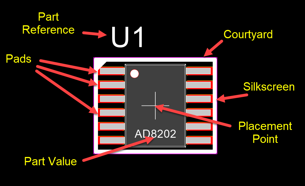
Footprints are the copper and silkscreen patterns (also called Land Patterns) that define the part on a PCB.
A footprint consists of:
•Pads
•The Footprint Placement Point