In the realm of printed circuit board (PCB) design, a pad is a specific area of copper on a PCB layout that allows for the soldering of component leads or pins. Pads are fundamental to establishing electrical connections between the PCB's traces (circuit paths) and the components.
There are various types of pads used in PCB designs, depending on the type of component and the method of soldering:
•Through-Hole Pads: These are used for through-hole components. They are associated with drilled holes in the PCB where the component leads are inserted and then soldered. The pads might be on one side (single-sided boards) or both sides (double-sided boards) of the PCB.
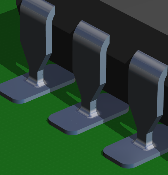
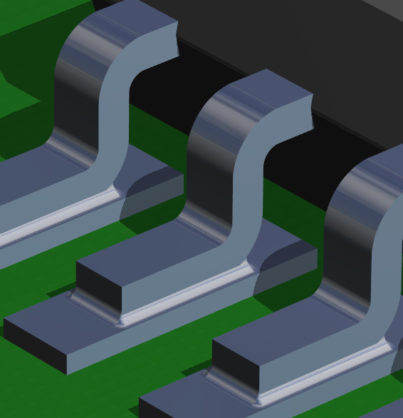
•Surface Mount Pads (SMD Pads): These are flat pads on the surface of the PCB where the leads or terminations of surface-mount components are soldered directly.
•Solder Paste Pads: For surface-mount technology (SMT) assembly where solder paste and reflow soldering are employed, pads can also define where solder paste should be applied using a stencil.
•Fiducial Pads: These are not for components but are reference points on the PCB. They are small, round copper areas used by automated assembly machines to align components accurately during placement.
•Test Pads: These are designed to be accessible points on a PCB for testing purposes. They provide a location where a test probe can make contact to check the function and characteristics of a circuit.
•Thermal Pads: These are larger pads often found underneath certain components, such as power ICs, to help dissipate heat. They can be connected to ground or other planes to aid in thermal management.
•Castellated Pads or Half Pads: These are seen on module PCBs where the edge of the PCB is milled to create half-moon shaped pads. This design allows the module to be soldered onto another PCB, similar to an SMD component.
A few other considerations related to PCB pads:
•Size: The pad size is crucial. It needs to be large enough to allow for a good solder joint but not so large that it causes solder bridging or other defects.
•Shape: Pads can come in various shapes, such as rectangular, round, or oblong, depending on the component lead shape and the designer's preference.
•Spacing: The distance between pads, especially for ICs with many pins, is critical to prevent solder bridging and to adhere to the specifications of the component.
•Annular Ring: For through-hole pads, the annular ring is the portion of the pad that surrounds the drilled hole. It's essential for ensuring a solid solder connection.
Proper pad design is essential for the manufacturability, reliability, and performance of a PCB. Many PCB design tools come with libraries of standard footprints, which include predefined pad sizes and shapes for common components, ensuring that these criteria are met.
Electrical parts are 'glued' on the PCB using solder between the part's electrical terminals and copper pads on the PCB. The solder is usually the only way the part is mechanically affixed to the PCB.
 TPH Pads Soldered (glued) to PCB |
 SMT Pads Soldered (glued) to PCB |
Pad are copper areas on the top/bottom or both sides of the PCB.
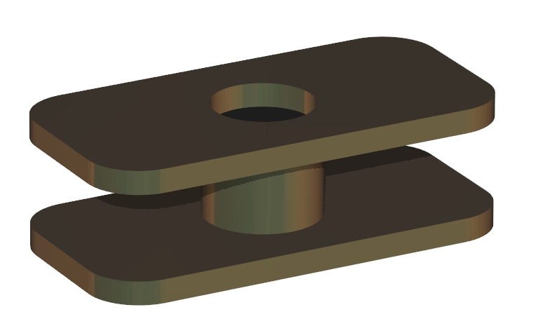 TPH Pad (PCB invisible) |
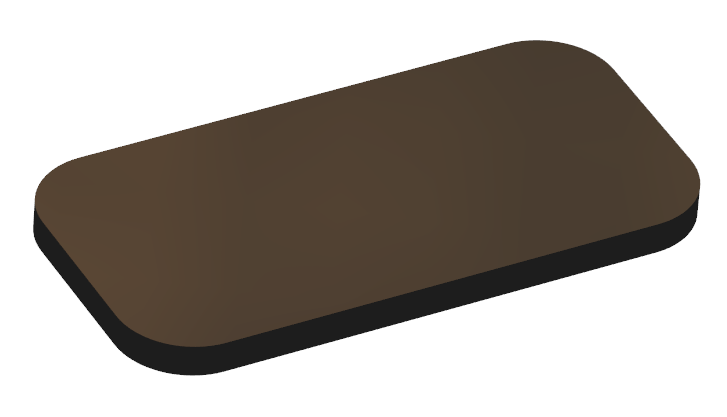 SMT Pad (PCB invisible) |
If pads are on both sides then there is a hole drilled trough both the top and the bottom side of PCB and is usually plated with copper to provide an electrical connection between both sides.