Pads can be circular, elliptical, rectangular (with optional rounded corners) polygonal or a complex curve.
PCB pad shapes are chosen based on several factors, including the component lead geometry, soldering method, manufacturability, and specific requirements of a design. While there's a variety of pad shapes used in PCB designs, here are some of the most common ones:
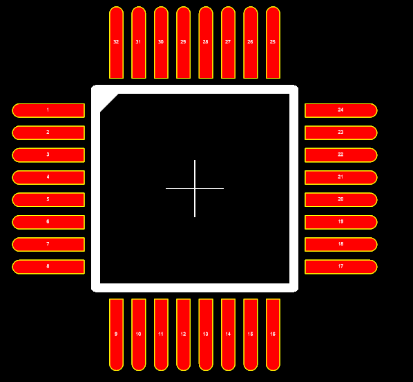
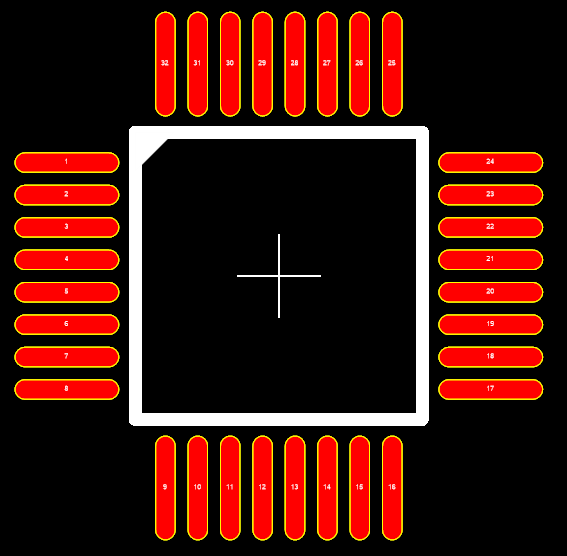
•Rectangular Pads: These are perhaps the most common type of pads, especially for surface-mount devices (SMD). They're often used for ICs, resistors, and capacitors.
•Round Pads: These are typically used for through-hole components and some types of connectors. They can also be employed as test points or fiducial markers.
•Oblong (or Oval) Pads: These are a hybrid between rectangular and round pads and are commonly used for certain SMD components, like tantalum capacitors, or for certain types of connectors.
•Square Pads: While less common than rectangular pads, square pads can sometimes be used to indicate pin 1 of an IC or to differentiate a specific pin from others.
•D-Shaped (or C-Shaped) Pads: This unique shape can be employed for alignment purposes or to ensure correct orientation for components that need to be placed in a particular direction.
•Polygonal Pads: Sometimes, custom-shaped pads are necessary, especially for certain connectors or specialized components. These pads can take on a variety of polygonal shapes.
•Thermal Pads: These are often large square or rectangular pads found underneath certain components like power ICs. They're used to facilitate heat dissipation and may have multiple vias within them to improve thermal performance.
•Solder-Thieving Pads: These are pads strategically placed at the ends of rows of pads (e.g., on fine-pitch ICs) to "thieve" or attract excess solder. Their goal is to reduce the likelihood of solder bridging between closely spaced pads.
•Castellated Half-Circle Pads: Found on the edges of module PCBs, these half-circle (or semi-circular) pads allow the module to be soldered onto another PCB as though it were an SMD component.
The choice of pad shape affects several aspects of the PCB:
•Solderability: The pad shape can influence how easily a component can be soldered onto the board, especially during automated soldering processes.
•Mechanical Strength: Some pad shapes may offer better mechanical strength, especially under mechanical stress or during thermal cycling.
•Visual Inspection: Different pad shapes might make visual inspection processes easier or harder, depending on the contrast they provide against soldered component leads.
•Real Estate: On densely populated boards, the shape and arrangement of pads can influence how many components can fit in a given area.
When designing PCBs, engineers will often rely on component libraries in their PCB design software. These libraries usually contain predefined footprints with optimized pad shapes for various components. However, designers can also create custom pad shapes when necessary to meet specific requirements.
Circular |
 Elliptical |
 Square |
 Rectangular |
 Rectangular with rounded corners |
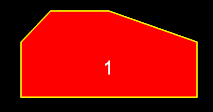 Polygonal |
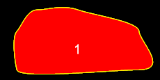 Curved |
In addition Pads in rectangular parametric footprints can have rounded corners set to sides.
 |
 |
 |