The anatomy of a PCB (Printed Circuit Board) design refers to the various components and layers involved in creating a functional PCB. Understanding the structure and elements of PCB design is essential for engineers and designers to ensure that the board meets electrical, mechanical, and thermal requirements. Here’s a detailed overview of the key components of PCB design:
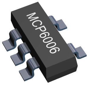
For AutoTRAX DEX, a part can be one of several different things. These are physical parts, which can either be electrical or purely mechanical and non-physical parts which can also be electrical but can also be meta data such as sheet title blocks or just graphics.

A Typical Part
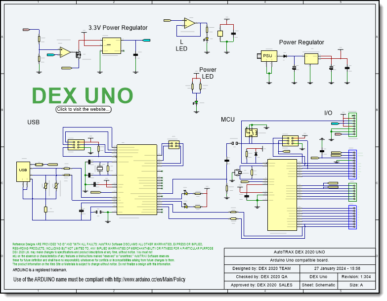
Schematics are detailed diagrams that represent the electrical connections and functionality of a circuit used in the design of a printed circuit board (PCB). These schematics depict how components such as resistors, capacitors, transistors, integrated circuits, and other devices are interconnected using symbols and lines, which represent the electrical connections (nets) between them.

A Typical Schematic
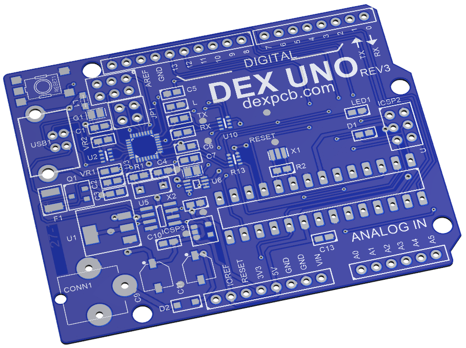
The PCB is the physical manifestation of your design and represents your ultimate goal - To make a PCB.

A Typical PCB with no Parts