To produce a cost-effective layout through optimum PCB material usage, you are recommended to consult with your PCB manufacturer to determine the optimum panel size. The PCB should be design to utilize the manufacturers suggested usable area. Smaller PCBs may be ganged of red in the uniform apparel format to simplify fixture and reduce excessive angling during assembly.
The main reason for having your boards delivered in an array is to make automated assembly faster and less expensive. Running an array of boards through a pick-and-place machine is far more efficient than sending them through one at a time. Arrays are also desirable because they allow the addition of tooling rails, tooling holes, and fiducials, all of which help your assembler.
Tooling Rails are the 'holding frame' for the array. They provide stability and make it easier to handle the arrays throughout the assembly process. Tooling holes and fiducials are usually added to the tooling rails.
Tooling Holes are non-plated holes added to the rails so the array can be pinned down to prevent unwanted shifting during assembly. They are typically 0.125" in diameter but can be drilled to your required specification.
Fiducials are copper markers on the rails, which aid automated pick-and-place assembly equipment by providing a uniform reference point. The copper fiducial is typically 0.04" in diameter and will not be covered with mask to make it easier for assembly equipment to see.
A PCB panel may include several into circuit boards arranged in a matrix or simply one printer circuit board requiring additional material retained for efficient assembly. The large PCB are several smaller PCBs are retained in the panel separated after all assembly is completed. Separating the individual PCBs from the panel can be done using several methods which include the – will scarring, and see routing and slotted routes with breakaway tabs.
What type of array to use?
There are 3 types of arrays:
1.Scored
2.Tab Routed
3.A mixture of both.
So how do you decide which one is right for your design?
Scoring is the preferred choice for two reasons.
1.Scoring has the advantage of a more consistently smooth board edge,
2.and it wastes less material, which can mean cost savings especially for larger quantities or high layer count printed circuit boards where every square inch counts.
You should consider tab routing when your design has an irregular shape or if you need space between your boards to allow for overhanging components.
A mix of scoring and tab routing can be used when some board sides are straight, which can be scored, while irregular sides must be tab routed.
There are two ways to create PCB Breakaway Panels.
•Mouse bites (a.k.a. breakaway This is a test of the font height tab on routing)
•V – score (a.k.a. V–Grove)
V–Groves are cuts, usually on both sides of a PCB and generally in a straight line. They are made with a cutter with a cut angle of 30° or 45°
You need tooling rails along the two longest sides and there should be no space between the boards. The score will be made along the shared board outline. Scoring is performed only parallel to the x- and y-axes, not diagonally. Because scoring runs all the way across the array in a straight line, the board outline should be straight for scored arrays.
The score depth is approximately ⅓ of the total material thickness. Score lines will be made on the top and bottom sides of the PCB. This will leave a remaining web of material equal to approximately ⅓ of the total thickness of the board. If your board is1mm thick, the remaining material will be ~0..33mm.
Standard PCB material is basically fiberglass. Even though your board is scored, it will still be sturdy so be careful when separating the boards. You should expect some amount of flexing before the score line will give. Some fiberglass strands are common along a scored edge. A quick skim with a sander will take care of any rough areas.
Jump Scoring
It is possible to stop a score from continuing all the way across an array; this is referred to as jump scoring. However, this is not a recommended array solution due to the limitations and expense of this process. We strongly encourage the use of tab routing rather than jump scoring.
Scoring cannot be stopped precisely enough to end a score line like a CNC route. To make a complete score, the scoring blade must travel past the end point and come to a stop. You need a minimum of a 7 mm gap between the stop score location and anything that is not intended to be scored.
If your design has an irregular shape, then tab routing may be required. AutoTRAX DEX will add a gap, equal to the router cut width, between the boards to allow the router bit to pass between them. Small tabs of material will remain to hold the boards in place. To make separation easier, you can add small non-plated holes to the tabs called 'mouse bites to perforate the tab. If you desire a smooth edge on your PCBs, these areas will need to be sanded after the boards are removed from the array.
Because tab routed arrays are inherently less sturdy than scored arrays,You should add tooling rails to all 4 sides of the array. This will give your array of PCBs more support during handling and assembly processes.
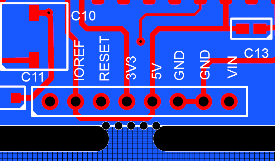
Mouse Bites
Each break-out tab has it's own set of 5 automatically created mouse-bite holes.
Break-apart tab with mouse-bites
Breakout
The spacing between breakaway tabs can range from 60 mm to 90 mm, but the IPC recommend 75mm or 3" . Try not to exceed 100 mm between tabs and try to evenly space them apart.