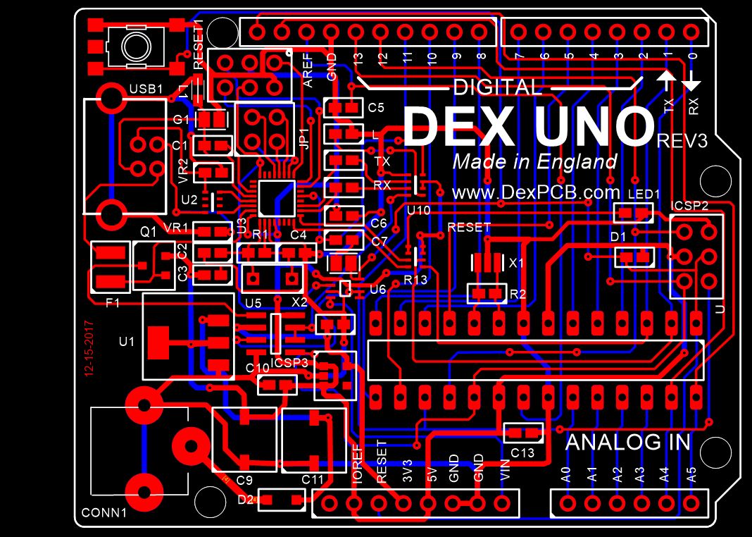
The PCB is the physical manifestation of your design and represents your ultimate goal - To make a PCB.

A typical PCB

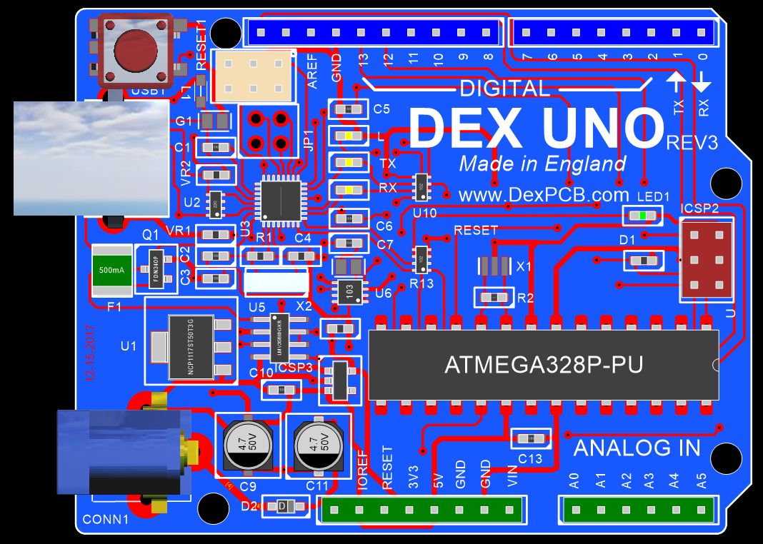
The PCB showing the PCB filled and physical parts on the top of the PCB

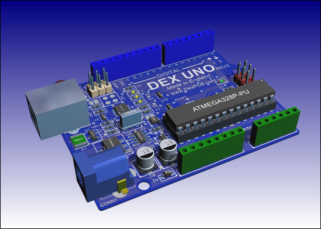
The PCB viewed in 3-D
It consists of a PCB border, parts and electrical connections.
A PCB border
The border can have any number of cutouts and round hole. Cutouts are usually created with a CNC cutter and are expensive. Round holes are simply drill out.
Parts
You place the footprints for your physical parts inside the border and usually not covering holes and cutouts. However, sometimes you may place a part over a cutout/hole so design reasons.
Parts can be placed on the top or the bottom of the PCB.
The parts are connected together either by electrical copper tracks or via internal layers of solid copper called signal/power planes.
Copper Tracks (electrical connections)
Tracks are parts of electrical PCB nets.
A Net is a collection of pads that need to be electrically connected together. AutoTRAX DEX calculate a optimal unrouted non-cyclic* graph of unrouted track.
Nets map 1: 1 with schematic nodes.
You manually route the unrouted tracks. That's the fun part. You can also use an auto-router.
*non-cyclic - does not form loops
A printed circuit board, or PCB, is used to mechanically support and electrically connect electronic components using conductive pathways, tracks or signal traces etched from copper sheets laminated onto a non-conductive substrate. When the board has only copper tracks and features, and no circuit elements such as capacitors, resistors or active devices have been manufactured into the actual substrate of the board, it is more correctly referred to as printed wiring board (PWB) or etched wiring board. Use of the term PWB or printed wiring board although more accurate and distinct from what would be known as a true printed circuit board, has generally fallen by the wayside for many people as the distinction between circuit and wiring has become blurred. Today printed wiring (circuit) boards are used in virtually all but the simplest commercially produced electronic devices, and allow fully automated assembly processes that were not possible or practical in earlier era tag type circuit assembly processes.
A printed circuit board (PCB) mechanically supports and electrically connects electronic components or electrical components using conductive tracks, pads and other features etched from one or more sheet layers of copper laminated onto and/or between sheet layers of a non-conductive substrate. Components are generally soldered onto the PCB to both electrically connect and mechanically fasten them to it.
Printed circuit boards are used in all but the simplest electronic products. They are also used in some electrical products, such as passive switch boxes.
PCBs can be single-sided (one copper layer), double-sided (two copper layers on both sides of one substrate layer), or multi-layer (outer and inner layers of copper, alternating with layers of substrate). Multi-layer PCBs allow for much higher component density, because circuit traces on the inner layers would otherwise take up surface space between components. The rise in popularity of multilayer PCBs with more than two, and especially with more than four, copper planes was concurrent with the adoption of surface mount technology. However, multilayer PCBs make repair, analysis, and field modification of circuits much more difficult and usually impractical.
A PCB populated with electronic components is called a printed circuit assembly (PCA), printed circuit board assembly or PCB Assembly (PCBA). In informal use the term "PCB" is used both for bare and assembled boards, the context clarifying the meaning.