You can add copper pour areas to your PCB.
The term "copper pour" refers to an area on a printed circuit board filled with copper (the metal used to make connections in printed circuit boards). Copper pour is commonly used to create a power or ground plane. Another reason for using copper pour is to reduce the amount of etching fluid used during manufacturing.
A distinctive feature of copper pour is the back-off/margin (or stand-off) - a certain distance between the copper pour and any tracks or pads not belonging to the same electrical net. A copper pour therefore looks like it flows around other components, with the exception of pads which are connected to the copper pour using thermal connections.
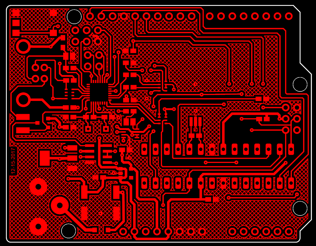
While solid copper pour provides better resistive characteristics, hatched copper pour is used to balance the heat and open space on both sides of the board in order to avoid warping of certain substrates. Heating might cause gas bubbles between solid copper pour and certain substrates. Furthermore, it might be possible to adjust the impedance of high frequency traces by using hatched copper pour in order to reach better signal quality.
Copper Pour Area