Whats New for 2023
December
Saturday 30 December 2023
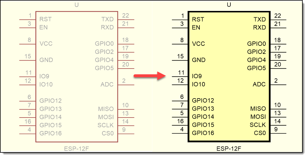
![]() User Interface - Footprint Builder Panel
User Interface - Footprint Builder Panel
•DIP switch and LED - no material settable in 3D.
•DIP footprint dialog size - removed empty/disabled/unused controls.
•Part type - Display in 3D option did not work.
•Moving part type entities caused flicker in part type color chooser.
•Crystal footprint dialog layout improved.
Thursday 28 December 2023
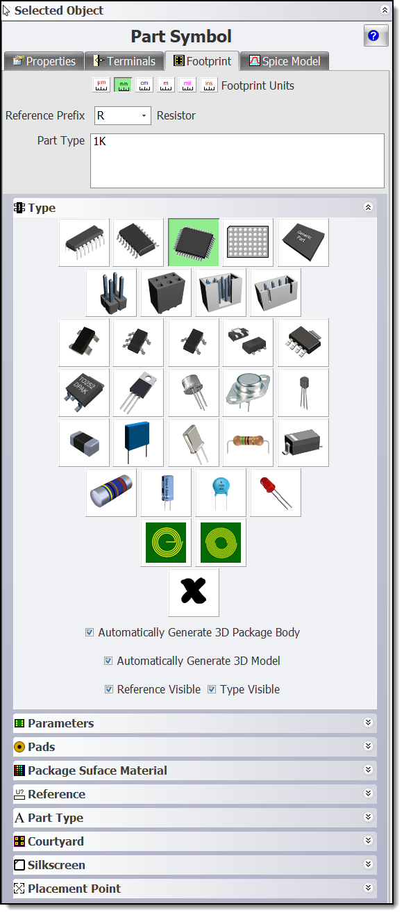
New Part Dialog
Added all the features available in the Part Builder panel.

New Part Dialog
Wednesday 27 December 2023
Part Builder Panel
Improved interactive behavior with the viewports when modifying properties.
Parametric Parts: An Overview
This tutorial video gives you a quick overview on creating parametric parts.
An Overview of Parametric Parts
Tuesday 26 December 2023
Part Builder
Improved behavior when selecting different parametric part types in Part Edit mode.
Saturday 22 December 2023
Multiples 3D Viewports
Improved interaction with the Part Builder.

Multiple 3D Views
Friday 22 December 2023
![]() User Interface - Part Builder and Properties Panels
User Interface - Part Builder and Properties Panels
•Fix for 'flashing color' chooser. Control displays more persistent. Removed empty spaces.
•Fix for top texture on DIP 3D packages.

DIP with Texture
Thursday 21 December 2023
Pin Material for MELF Parts
You can now set the pin materials for MELF parts.
 Dull Silver |
 Silver |
 Dull Gold |
 Gold |
Wednesday 20 December 2023
Copper Pours and Split Power Planes
Placing copper pours or split power planes on inner layers prevents the inner layer from being a signal/power plane.
Smart Pads with Automatic 3D Generation

Automatic 3D Generation

Pad Editor
Tuesday 19 December 2023
![]() Internal Code Optimization and User Interface Optimization/Layout.
Internal Code Optimization and User Interface Optimization/Layout.
Sunday 17 December 2023
Auto-Position
New properties check-box for automatically setting the position for footprint part types, references, and placement points.
 Footprint Part Type |
 Footprint Reference |
 Footprint Placement Point |
Saturday 9 December 2023
Shortcut Keys - Productivity Aids
New shortcuts.
The Zoom Window key ('5' with nums lock turned off) will make your life so much easier. Try it!

Zoom Window
")
Zoom Window (nums lock turned off)
")
Zoom Content (nums lock turned off)
")
Home View (nums lock turned off)
")
End Current Command (nums lock turned off)
•Thursday 7 December 2023
Improved New Parametric Part Dialog
•You can now add a datasheet.
•Symbol terminal captures works from added datasheet.
Create a LM321 Op-Amp Parametric Part

New Parametric Part Dialog
This tutorial video on creating parametric parts in DEX, a software tool for electronic design. The speaker guides the viewer through the process of creating a part for an operational amplifier (LM321) using DEX's parametric parts dialogue. The steps include:
1.Starting a New Project: Opening DEX and making sure the home ribbon tab is visible.
2.Creating a New Part: Clicking on the parametric part button to display electronic part symbols.
3.Selecting a Part to Create: Choosing to create a part for the LM321 Single Channel Operational Amplifier.
4.Referencing the Datasheet: Locating and opening the datasheet for the LM321.
5.Adding the Datasheet to the Design: Embedding the datasheet into the part file.
6.Selecting the Physical Package: Choosing the SOT23−5 package from the parametric parts collection.
7.Creating Footprint, Symbol, and 3D Model: Auto-generating these elements based on the chosen package.
8.Assigning Names to Symbol Terminals: Using the capture feature to assign names to the symbol terminals based on the datasheet.
9.Finalizing the Design: Setting the part type and creating the part for further editing.
10. Saving the Part: Using the library panel to save the part in the desired directory.
11.Using the Created Part: Demonstrating how to use the newly created part in a new project.
The video emphasizes the importance of practice, exploring available options, and the impact of quality parts on the overall design. The tutorial is meant to make the process of creating parts in DEX more efficient and enjoyable.
Monday 4 December 2023
![]() Internal Array Indices Errors
Internal Array Indices Errors
Fixed index out of bounds errors. These were previously caught, but now are prevented from happening.
November
Thursday 30 November 2023
Rotating PCB parts
You can now rotate PCB parts, including the PCB Border, and tracks provided none of the selected objects is locked.

Rotated PCB
Monday 27 November 2023
Eagle Parts - Import
Improved symbols
 Symbol |
 Footprint |
Sunday 19 November 2023
Parametric Parts
Improved automatic 3D models.
Design Rule Checker
More comprehensive error messages.
Thursday 16 November 2023
Schematic Wire Appearance, Junctions and Cross-overs
This demonstration video shows you how to customise the appearance of the wires in your schematics.
Schematic Wire Appearance
Resizing Using the Thumbwheel
When it comes to editing your designs, there's often a need to swiftly adjust the width or size of various elements. In DEX, you can achieve this effortlessly using the middle thumbwheel on your mouse. This video demonstrates how you can change track widths, via diameters, and pad sizes in your PCB design.
Resizing Using the Thumbwheel
Sunday 7 November 2023
Finding Symbols and Footprint in Your Design Using the Navigator Panel
The Navigator Panel
In complex designs, navigating and locating components within schematics and PCB layouts can be challenging. DEX provides a powerful feature to simplify this process: the Navigator Panel. In this tutorial, I'll demonstrate how to effectively utilize the Navigator Panel to find your symbols in schematics and the corresponding footprints on the PCB.
Using the Router Panel When PCB Routing
The Route Panel
When designing the PCB, it is vital that you know where the electrical connections are and to which footprint pads they are connected to. At the same time, it is also very useful to see statistics about each individual PCB net. This is where DEX Router panel comes to your rescue.
This tutorial video will demonstrate the usefulness of the router panel.
Saturday 4 November 2023
Checklist
The Checklist Panel
After you have completed the design of your schematic, you must, absolutely must, check it. There is a saying among joiners “measure twice, cut once.” Mistakes in your design at this stage are far easier and cheaper to correct than design mistakes detected when you receive your first prototype boards.
DEX has several powerful utilities that help you check your design and make sure it is okay for manufacture. The design tool I am going to discuss in this video is the checklist panel.
Added ![]() Button. See video.
Button. See video.

Checklist Panel
Friday 3 November 2023
Adding and Editing Arcs in Schematics
Adding and Editing Arcs in Schematics
In this tutorial video I am going to show how to add arcs visually using the mouse and the viewport.
I will also show you how to edit lines using either the mouse or by numerical entry.
Finally I will show you how to edit many of the properties of an arc using the arcs property panel.
Wednesday 1 November 2023
![]() Internal Data Checks
Internal Data Checks
•Added extra internal data consistency checks with auto-repair. These checks are done automatically when DEX starts and you do not need to run them manually.
•The checks include:
•Entities being on the wrong sheet such as symbols being on PCBs!
•Entities that will be invisible such as lines with the same starting endpoint, and circles and ellipse with zero diameter.
October
Saturday 28 October 2023
Setting Hole Diameter of All TPH Pads
You can set the hole diameters of all TPH pads using the PCB properties in the Properties Panel - Sheet Editor

Properties Panel - Sheet Editor

Setting Hole Diameter of All TPH Pads
Friday 27 October 2023
Faster Opening of Large Projects
Tuesday 24 October 2023
Import Eagle Design Rule Files
You can now import Eagle DRC files. These are often supplied by PCB manufacturers such as PCBWay

Import Design Rules
![]()
PCB Drill Holes
•Fixed 3D view where some holes did not appear.
•Default minimum drill hole size set to 0.15mm.
Sunday 22 October 2023
New 'Send Feedback' and 'Wish list' Dialogs
Experience a streamlined way of sharing your insights and desires through our newly integrated dialog features. Gone are the days of being redirected to web pages. Now, these dedicated dialogs within DEX enable you to directly paste images, format text, and reference the open project, simplifying the way you communicate your ideas.
We've prioritized the security of your communications, ensuring a protected channel for your feedback and requests.
We encourage you to utilize these features, as your valuable insights are instrumental in refining DEX. By sharing your experience, you're contributing to an improved platform not just for your benefit, but for the entire DEX community.

'Send Feedback' and 'Wish List' buttons

Send Feedback Dialog
Wednesday 18 October 2023
From Concept to Creation: Mastering PCB Design
"From Concept to Creation: Mastering PCB Design" is a comprehensive guide or course focusing on the journey an electronics engineer undertakes, from theoretical aspects of PCB (Printed Circuit Board) design to the practical elements of bringing a concept into a tangible, functional PCB. This guide would not only equip you with theoretical knowledge needed to understand PCB design but also the practical skills you need to take a project from an idea to a physical, working product. It’s the comprehensive journey from learning the ropes of electronics to mastering the art and science of PCB design.
From Concept to Creation: Mastering PCB Design
Monday 16 October 2023
User Forum
DEX User Forum has now returned to https: //forum.dexpcb.com
You can access DEX User Forum by clicking on the Help →  button in DEX Ribbon menu.
DEX User's Forum is an online platform or community where users of DEX can come together to discuss, share, and seek support on various aspects of using the software.
This forum provide a place for you to:
•Share tips and tricks about using the software that they have discovered.
•Provide tutorials or guidance to new users or those facing difficulties.
•Discuss bugs or issues with the software and sometimes receive support from the company itself or experienced users.
•Request new features or modifications, which companies often use for feedback for new versions.
•Share design samples, tools, or libraries that they have created, which can be beneficial for others working on similar projects.
This kind of forum is immensely beneficial in niches like electronic design software because they foster a community of practice that can enhance the professional or hobbyist pursuits of their members. However, the specifics, rules, and offerings of each forum can vary, and you'd need to access DEX User's Forum directly to understand its particular structure and content.
Thursday 12 October 2023
Website
DEX website has now returned to https://dexpcb.com
It was using https://dexpcb.com
Monday 9 October 2023
Manual
Improved larger font sizes.
Monday 9 October 2023
Manual
Improved larger font sizes.
![]() Adding Symbol Terminals in Projects
Adding Symbol Terminals in Projects
Add terminal buttons were not visible.

Add Symbol Terminal Buttons
Saturday 7 October 2023
New Capture Screen Area

Capture Screen Area
![]()
Resistor Color Band
Fix for out of range color bands.

Resistor Color Bands
Tuesday 3 October 2023
![]()
SOT Parametric Parts
Fix for pin layout.

SOT-23-3
Axial Parametric Parts
Fix for text on side of vertical parts in 3D.

Axial Parametric Part
Images in 3D
Fix for transparent pixels showing shadows.
Fix for orientation on the image on the bottom side.

3D Image
Sunday 1 October 2023
How to Import a 3D STEP file

Importing a STEP into DEX
Improved Import 3D Dialog
Improved viewing.
Double click on the 3D viewport to view the 3D fullscreen.

Import 3D Dialog
September
Saturday 16 August 2023
Adding STEP 3D Models
Currently, DEX does not support directly importing STEP 3D files.

FreeCAD with Imported USB STEP File
However, you can import a STEP file by:
1.importing it into FreeCAD, then
2.exporting it as a Collada file,then
3.Import the Collada file into DEX.
Saturday 9 August 2023
Autosize Vias
You can now automatically size track vias based on the maximum width of the connected tracks and the minimum/maximum via sizes settings.
•Via hole diameter = maximum width of the connected tracks taking into account the minimum and maximum via hole sizes - see settings.
•Via diameter = twice the via hole diameter.
Maximum and Minimum Via Hole Sizes
The maximum and minimum via hole sizes in a printed circuit board (PCB) can vary depending on the specific requirements of the design and the capabilities of the PCB manufacturer. However, I can provide you with typical ranges for both maximum and minimum via hole sizes:
Minimum Via Hole Size
•The minimum via hole size is often determined by the manufacturing process and the capabilities of the PCB manufacturer.
•For standard PCB fabrication processes, the minimum via hole size can be as small as 0.1 mm (100 micrometers) or even smaller.
•Miniaturization trends in electronics have led to the development of advanced techniques that can create even smaller microvias with sizes in the range of 0.05 mm (50 micrometers) or less.
Maximum Via Hole Size
•The maximum via hole size is less constrained by manufacturing processes compared to the minimum size.
•For most standard PCBs, the maximum via hole size is typically determined by the size of the components and the available space on the board. In such cases, it can be several millimeters in diameter.
•For specialized applications, where larger vias are needed to carry high currents or for other specific purposes, custom sizes can be accommodated, and the maximum size can be much larger, exceeding 10 mm or more in diameter.
It's important to note that while these are typical ranges, the actual minimum and maximum via hole sizes for a specific PCB design should be discussed with the PCB manufacturer, as their capabilities and equipment may vary. Additionally, the choice of via hole size should consider the electrical and thermal requirements of your design, as well as the space available on the PCB. Custom requirements may incur additional costs, so it's essential to work closely with your manufacturer to ensure your design needs are met effectively.

Autosize Vias

Before Auto-setting Via Sizes

After Auto-setting Via Sizes
PCB Cutout Arc
You can now add PCB cutout arcs.

Add PCB Cutout Arc Command

3 PCB Arc Cutouts

3 PCB Arc Cutouts in 3D
Tuesday 5 August 2023
![]() Plotting
Plotting
Fix for solder-mask layers not plotting correctly. Gerber and printing were OK.
August
Thursday 31 August 2023
![]() Plotting
Plotting
Fix for solder-mask layers not plotting correctly. Gerber and printing were OK.
Tuesday 29 August 2023
![]() Rebuilding Parametric Footprint from Presets
Rebuilding Parametric Footprint from Presets
Fix for initial silkscreen position error.

Rebuilding a Parametric Footprint from Presets
Monday 28 August 2023
Small Outline Diodes

Create Parametric Parts
Sunday 27 August 2023
Small Outline Diodes
"SOD" stands for "Small Outline Diode" or "Small Outline Diode package." It's a package style commonly used for surface-mount diodes, particularly small signal diodes and Schottky diodes. SOD packages come in various sizes, each identified by a number such as SOD-123, SOD-323, SOD-523, and so on. These package styles are standardized and are designed to be compact and suitable for automated assembly processes.
Here are a few examples of SOD package types:
•SOD-123: This is a common SOD package size for small signal diodes. It has two leads and is typically used for low-power diodes.
•SOD-323 (also known as SC-76): SOD-323 is slightly smaller than SOD-123 and is used for smaller, low-power diodes.
•SOD-523 (also known as SC-79): This is even smaller than SOD-323 and is often used for miniature signal diodes.
 SOD with Flat Leads |
 SOD with Gull Wing Leads |
New parametric parts for:
•SOD-323
SOD-323 is a type of surface-mount diode package. Surface-mount technology (SMT) is a method for producing electronic circuits in which the components are mounted directly onto the surface of printed circuit boards (PCBs). SOD-323 is one of the package types used for small signal diodes and other small electronic components in SMT applications.
Key characteristics of the SOD323 package include its small size and flat rectangular shape, which makes it suitable for use in compact electronic devices. The SOD-323 package typically has two leads that extend from the sides of the package, allowing it to be soldered directly onto the PCB. This eliminates the need for holes in the PCB, which was common in through-hole technology (THT) assembly.
SOD-323 diodes are often used in applications where space is limited, and high-frequency performance is required. They are commonly used for signal conditioning, voltage clamping, and rectification in various electronic circuits.

SOT-323
SOD-128

SOD-128
The SOD-128 is a type of surface-mount diode package. Like the previously mentioned SOD-323 package, SOD-128 is designed for small signal diodes and other electronic components in surface-mount technology (SMT) applications. However, the SOD-128 package is larger and has a different form factor compared to the SOD-323.
Key characteristics of the SOD-128 package include its flat, rectangular shape and two leads that extend from the sides of the package. These leads are used for soldering the diode directly onto the surface of a printed circuit board (PCB), which is a hallmark of surface-mount technology.
The SOD-128 package is larger than the SOD-323, which means it can handle higher power levels and may be used in applications where higher current-carrying capacity is required. It's commonly used for rectification, voltage clamping, and other functions in various electronic circuits, especially those that need to handle moderate to high currents.
SOD-123
The SOD-123 is a popular surface-mount diode package used for small signal diodes and other similar semiconductor devices. It is widely used in various electronic applications due to its small size and compatibility with surface-mount technology (SMT) assembly processes.
Key characteristics of the SOD-123 package include:
Package Size: The SOD-123 package is relatively small and rectangular, making it suitable for compact electronic designs.
Lead Configuration: It typically has two leads extending from the sides of the package. These leads are designed for surface mounting onto a printed circuit board (PCB), eliminating the need for holes in the PCB.
Applications: SOD-123 diodes are commonly used for various functions in electronic circuits, including rectification, voltage clamping, signal conditioning, and protection.
Dimensions: The exact dimensions of the SOD-123 package may vary slightly depending on the manufacturer, but it generally falls within a standard size range.
Compatibility: The SOD-123 package is compatible with automated pick-and-place machines used in SMT assembly, making it suitable for high-volume production.

SOT-123
SOD-523
The SOD-523 is similar to the SOT-123.

SOT-523
SOD-923
The SOD-923 is similar to the SOT-123.

SOD-923
Saturday 16 August 2023
![]() Manual Routing
Manual Routing
Improved manual routing from SMT pads.
Wednesday 16 August 2023
![]() Fix for Courtyards and 3D Models in Footprints.
Fix for Courtyards and 3D Models in Footprints.
Fix for out of place 3D models and incorrect courtyards.
Tuesday 15 August 2023
![]() Bug Reporting
Bug Reporting
Bug reporter now works with larger files.
Monday 14 August 2023
Grid Size
Grid sizes now restricted to 0.1 = 1 inch. This prevents 'accidentally' setting grid spacing too small or too large and producing 'strange' behavior when creating, moving and sizing objects.
The Schematic Wiring Grid
In schematics and symbol schematic: in addition to the user defined snap grid, there is an internal fixed grid that is used for the schematic wire auto-router. This internal fixed grid is called the schematic wiring grid.
Wires and terminals always snap to this schematic wiring grid and changing the regular snap spacing and snaps per grid has no effect.
In schematics and symbol design, try not to think about inches or centimeters. Do not change the units or the general snap grid to metric; this will only confuse use. Restrict units to the PCB design and footprint design.
If you are using a schematic for other purposes that does not include adding parts, then you can ignore the schematic wiring grid and use whatever units you wish. The author has used schematics for planning office layout of furniture.

Schematic with a 0.05 Unit Grid
Schematics and part symbols schematics are unit-less. Read more about the Schematic Wiring Grid...
Plot Preview
Improved Plot Preview. Max pilot hole size added.

Plot Preview
The Saturn PCB Toolkit
The Saturn PCB Toolkit is a freeware resource for PCB related calculations.
It incorporates many features that PCB designers and engineers are in regular need of like current capacity of a PCB trace, via current, differential pairs and much more.
You can download it from here: https: //saturnpcb.com/saturn-pcb-toolkit/

Saturn PCB Design Toolkit
Saturday 12 August 2023
Automatic Sizing of PCB Vias
Each PCB net can optionally set all the via diameters and all the via hole diameters contained in the net.
The via diameter will be set to twice the track diameter and the via all diameter will be set to the hole diameter.
")
Track Context Menu (Right click)

Sheet Editor

Track Properties Menu
Thursday 10 August 2023
Courtyards
Improved behavior.
Tuesday 8 August 2023
![]() Page Size
Page Size
Fix for some page sizes not restoring on load.
Sunday 6 August 2023
Semi-transparent PCB, Fully Transparent PCB and Semi-Transparent Copper
Useful to aligning imported 3D models over pads.

3D Viewing Options

Moving Imported 3D Model to Align with Pads
Viewing from bottom with:
Shadows off, Semi-transparent copper, Fully transparent PCB.

Part

PCB
Thursday 3 August 2023
Internal Program Optimizations
Tuesday 1 August 2023
PCB - Toggle Net Visibility
When viewing the PCB, pressing the 'N' keys toggles the visibility of nets.
July
Monday 31 July 2023
Redesigned Dialogs

Add Resistor Dialog

Edit Resistor

Add Capacitor
Saturday 29 July 2023
![]() Hidden Grid and Guides
Hidden Grid and Guides
Fix for grid and guides not showing if View Panel checked in the PCB Panels properties panel.

PCB Panels Properties
Sunday 23 July 2023
Sample Projects
Updated the sample projects.

Sample 3D Project
Wednesday 19 July 2023
Ribbon Menu
All ribbon menu items now left adjusted. No menu items forced onto the right side of the ribbon menu. This makes it easier to locate buttons.
Monday 17 July 2023
Object Scale and Rotate Manipulators
Separation of control points has been increased to make manipulation easier.

Old Manipulator Spacing

New Manipulator Spacing
Sunday 16 July 2023
Manual
This manual now increased in size with loads of extra topics and information on designing PCBs: see the menu on the left. This manual now has over 200,000 words.
Download the Apple ePub manual
Saturday 8 July 2023
![]() Bug Fixes
Bug Fixes
Setting parametric footprint using parameters selector now keeps original part type.
Monday 3 July 2023
Setting Pen and Fill Colors Using the Color-bar
This video shows you how to set the pen and fill colours of selected entities in DEX.
It also shows you how to set the pen in full colours to be used when creating graphical entities.
Setting Pen and Fill Colors Using the Color-bar
June
Wednesday 28 June 2023
New Custom Snap Grid
Default for PCBs and Footprints.
![]() Bug Fixes/ Usability Improvements
Bug Fixes/ Usability Improvements
Several bug fixes, and usability improvement for custom part creation.
Sunday 25 June 2023
Creating Custom Part
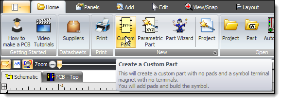
New ribbon menu to quickly create a new part without pads. You will use this to create a fully custom part rather than a parametric part.
You will manually add pads, optional custom 3D, and customize the symbol.
Tuesday 20 June 2023
![]() Footprint Values in 3D
Footprint Values in 3D
Fix for visibility in non-parametric parts.
Adding Graphical Lines
This video shows you how to quickly add lines to schematics in DEX.
It shows how you can add lines by defining the start and end points using the cursor or defining the starting points by entering numerical values using the keyboard.
Adding Graphical Lines
Editing Graphical Lines
You can set the line position, start and end points, width, colour, the start and end caps. And the line style.
Editing Graphical Lines
Friday 16 June 2023
Searching for Commands
This video shows you how to search for commands in DEX.
By simply entering text into the search command box, a list of commands that match your search twill be displayed.
Clicking on the command button will run the command.
Searching for Commands
Thursday 15 June 2023
Curve Manipulator
Improved visibility.
Wednesday 7 June 2023
Settings
Settings optimized and bugs fixed.
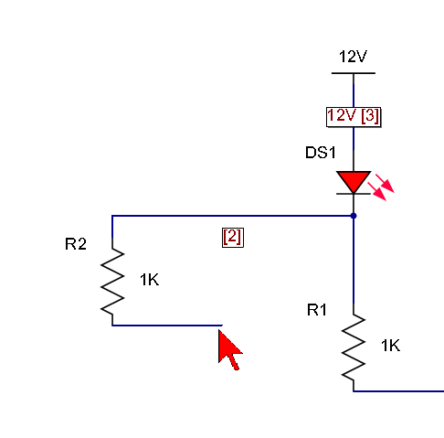
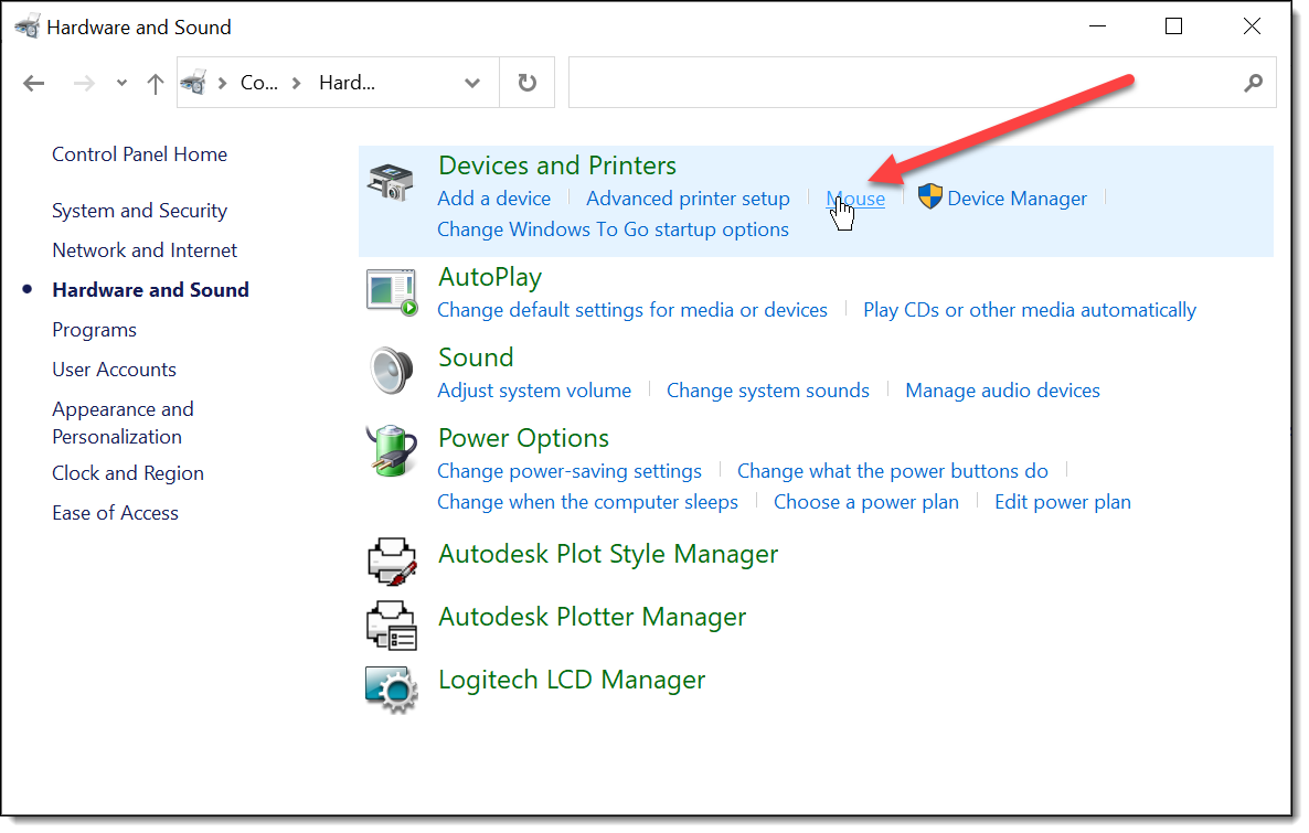
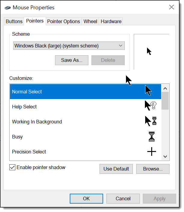
Cursors
Colored cursors.
Wednesday 7 June 2023
Cursors
You can now customize your cursors used in DEX using the Windows Control panel.
Monday 5 June 2023
Origin
The visibility of the origin is been greatly improved in both schematics and the PCB.
Schematic symbols
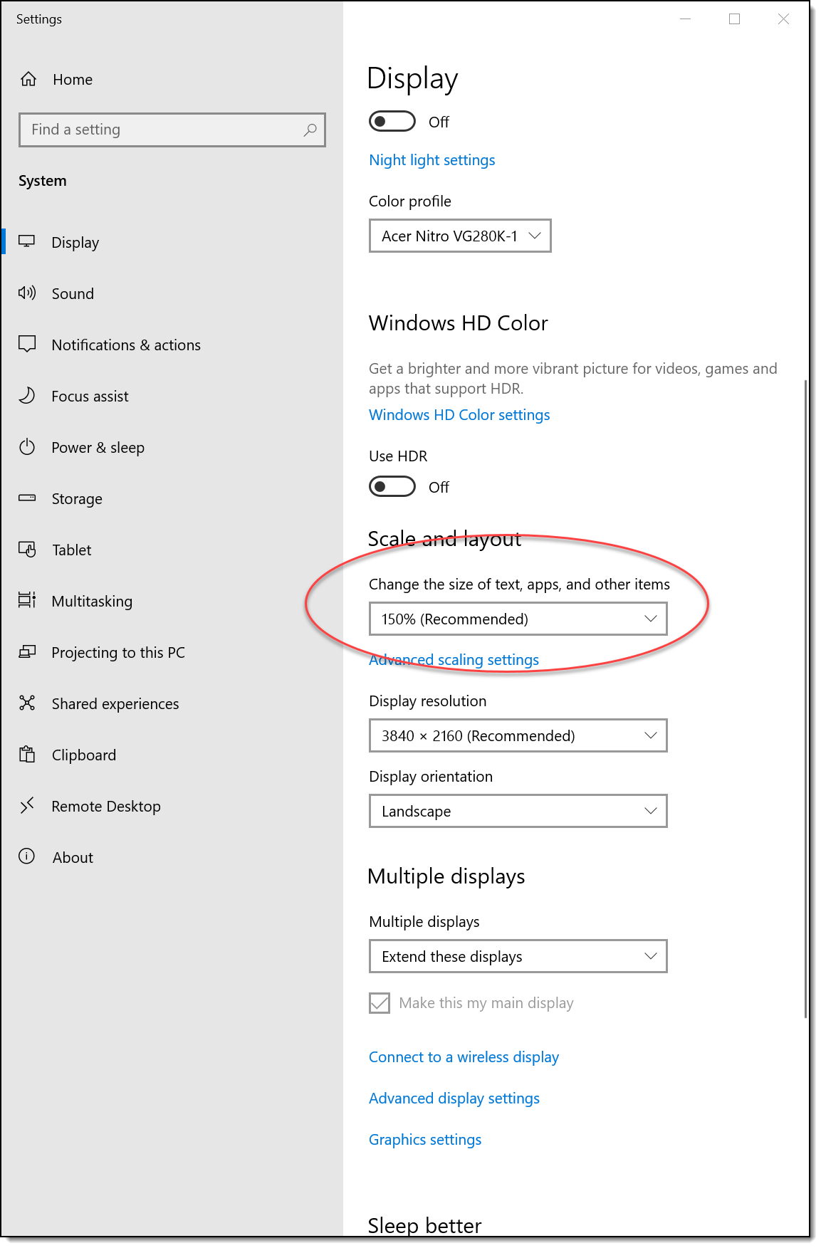
there was an error in the calculation of the over-strikes when the screen monitor has a text scale of greater than 100%. You will probably see this in 4K monitors where the text scale is typically set to 150%.

Saturday 2 June 2023
User Forum
Thursday 1 June 2023
![]() Missing Silkscreen Text in Gerber File
Missing Silkscreen Text in Gerber File
Fixed very rare occurrence of missing text in Gerber silkscreen files.
May
Sunday 28 May 2023
Code Optimization
Improved internal code and organization.
Sunday 21 May 2023
Buses
Improved editing in the viewport.
Friday 19 May 2023
Buses
You can now have multiple buses with the same name.
Beveled Bus Connections
Improved beveled bus connections.
Monday 1 May 2023
Resistors
Added Mega radio button to properties dialog.
April
Thursday 27 April 2023
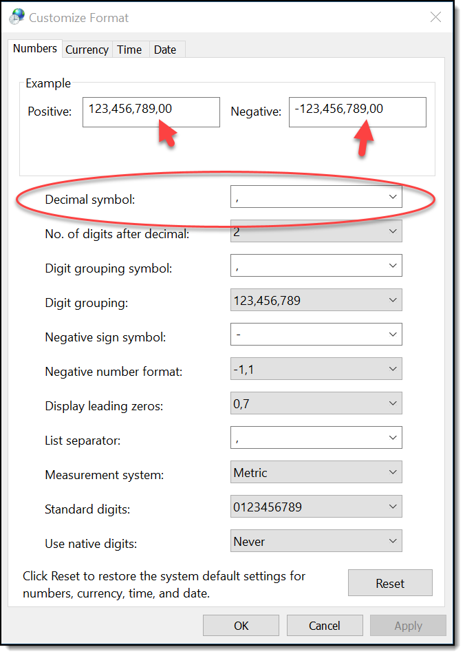
![]() Drill File Export
Drill File Export
Fixed error when local machine has Decimal symbol set to a comma.
Monday 24 April 2023
Internal Code Optimization
Improved quality of source code for DEX.
Sunday 23 April 2023
Navigator Panel
Improved sort order tro take into account sibling names.
![]() 2D Viewport in Fullscreen
2D Viewport in Fullscreen
Fixed view all using Home key: prevented slight zoom out after zoom all.
Tuesday 18 April 2023
Editor Control Layouts
More fine tuning of the layout of editors for monitor resolutions including 4K monitors.
Saturday 15 April 2023
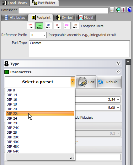
![]() Parameteric Part Preset Selector
Parameteric Part Preset Selector
Fixed.
Editor Control Layouts
The layout of controls in property editors and other editors has been improved and is more adaptive to screen resolution and text scaling.
Tuesday 11 April 2023
Popup Editor
No longer disappears after editing a single item. It remains open until you click on an area outside of it.
![]() Gerber Viewer
Gerber Viewer
Fix for scale error.
Monday 10 April 2023
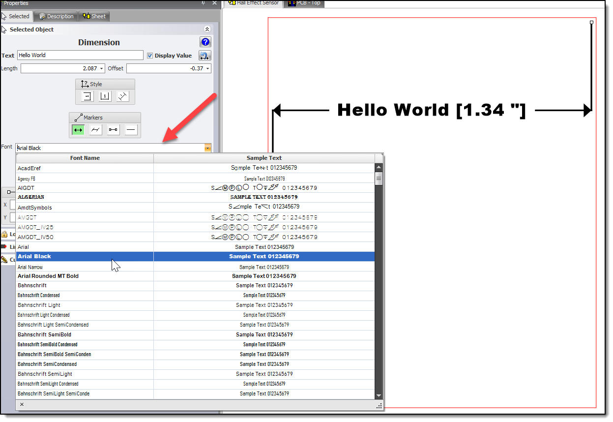
![]() Setting Fonts for Dimensions
Setting Fonts for Dimensions
Fixed.
![]() Property Value Editors Losing Focus
Property Value Editors Losing Focus
This caused the cursor to lose focus in number editors.
![]() Layers Panel
Layers Panel
Fixed layer colors not being drawn.
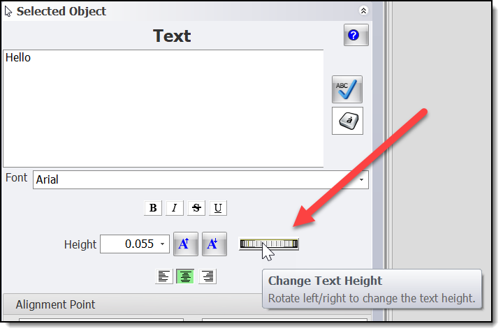
Text Height Thumbwheel
Sunday 9 April 2023
Part Type Text in 3D
Improved speed of 3D build.
![]() Symbol Part Type Text
Symbol Part Type Text
Fix for symbol part type text not updating during editing in the Properties panel.
Friday 7 April 2023
PCB Net Optimization
Automatic removal of track junction overlapping pads.
Zoom Content
Viewing content, for example pressing the Home key, sets view to maximize view of visible objects. Objects on layers that are turned off do not affect the view.
Thursday 6 April 2023
Real-Time Design Rule Checking
Improved speed for the Real-Time Design Rule Checking when manually routing. On large nets, such as power and ground nets, this can be over 100 times faster.
March
Sunday 26 March 2023
Manual Routing
Improved routing from SMT pads.
Saturday 25 March 2023
![]() Downloading Updates
Downloading Updates
Fix for problems with the new version downloading dialog 'hanging' and not downloading.
If you have this problem, please download direct from https://dexpcb.com/Download
Friday 17 March 2023
NC Drill Files
Format changed to make the output precision explicit; making it fully compatible with the Ucamco Reference Gerber viewer.
Thursday 16 March 2023
Improved Layout of Entity Properties Editors
Entity editors (for line, ellipses, arc etc.) improved layout.
Gerber Files
•Output precision increased to 1e-6 inches!
•Pad slot holes now correctly output.
•Gerber syntax improved to work with the Ucamco Reference Gerber viewer.
•Option to automatically open the Ucamco Reference Gerber viewer after outputting Gerber files.
![]() Left Ruler
Left Ruler
Fix for text labels not being drawn if viewing a PCB from the bottom.
Saturday 11 March 2023
What is DPI and why does it matter?
DPI stands for dots per inch, where a dot represents a physical device pixel. (The nomenclature comes from printing, where dots are the smallest ink dot that a printing process can produce). HDPI stands for high dots per inch.
Historically, monitors shipped with 96 pixels per inch. The Windows operating system drew a bitmap that represented 96 DPI as 100%. But as display technology progressed, that DPI threshold was surpassed. Monitors started shipping with display panels close to 300 DPI or higher.
While higher pixel density produces sharper images, some sort of display scaling is required to size elements on the screen properly. Otherwise, user interface (UI) elements and text are too tiny to use effectively and can overlap. To help remedy this, Windows automatically scales the UI percentile to match the DPI setting. For example, a DPI setting of 100% represents 96 DPI, where 125% is 120 DPI, and 150% is 144 DPI. This automatic scaling affects text, graphics, controls, and window sizes.
Here's where DPI-aware vs. DPI-unaware comes in. When an application declares itself to be DPI-aware, it's a statement specifying that the app behaves well at higher DPI settings and so Windows can apply auto-scaling. Conversely, DPI-unaware applications render at a fixed DPI value of 96 pixels per inch, or 100%, and so auto-scaling isn't applied.
DEX is now fully DPI-aware
Tuesday 7 March 2023
4K Monitors
Correct layout of popup panel contents with text scaling. (e.g. 150%)
Thursday 2 March 2023
4K Monitors
Correct layout of docking panel contents with text scaling. (e.g. 150%)
February
Monday 27 February, 2023
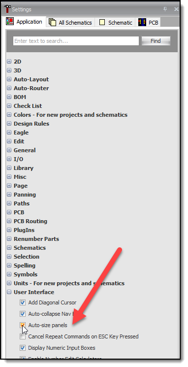
Docking and Floating Panels
DEX will now optionally adjust the width of docked panels and the size of floating panels so that the panel's controls are fully visible.
You can turn this off in the settings panel.
Wednesday 22 February, 2023
Docking and Floating Panels
Improved handling of minimum sizes of the panels.
Saturday 18 February, 2023
Sharper Text in 4K Monitors
Normally 4K Monitors scale text to say 150%. Previously this blurred text.
Previous
Now
Text scaling now works well.
Saturday 11 February, 2023
PCB Drawing Sometimes Slow
Fixed.
Sunday 29 January, 2023
January
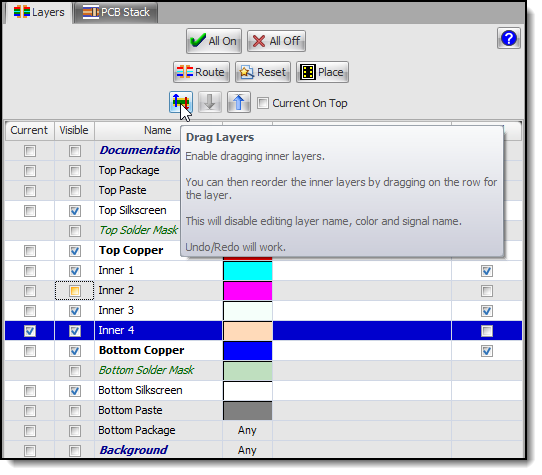
Moving Inner Layers Up/Down by Dragging
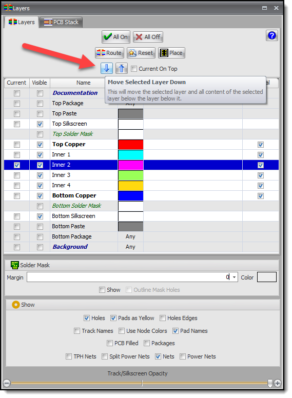
You can now drag the inner layer rows to alter their vertical ordering. This only works with boards with at least 2 inner layer.
Click the ![]() button. Then hold down the left mouse button over a layer's row and drag and release.
button. Then hold down the left mouse button over a layer's row and drag and release.
Dragging above or below the inner layers will move the dragged layer to the top/bottom of the inner layers.
Friday 27 January, 2023
Moving Inner Layers Up/Down
You can now move inner layers up/down the layer stack. This only works with boards with at least 2 inner layer.
Wednesday 25 January, 2023
![]() Eagle Import and BGA Parametric Footprints
Eagle Import and BGA Parametric Footprints
Fix for converting to parametric BGA footprint.
Saturday 21 January, 2023
Parts Catalog
•The quality of the parts in the parts catalog has been improved.
•There are now 54,260 parts.
•The right part preview windows have been improved.
•
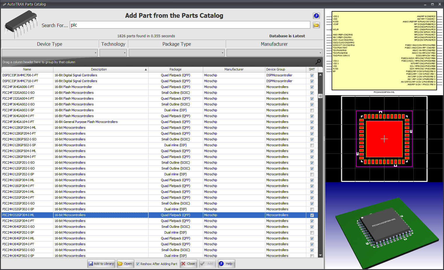
DEX will automatically download the new parts catalog to your machine.
Monday 16 January, 2023
SnapEDA Part Imports
Improved graphics for rectangles for SnapEDA parts.
Saturday 6 January, 2023
SnapEDA Part Imports
Improved graphics for symbols for SnapEDA parts.
Downloading Parts from SnapEDA.com
You can now easily search for parts on SnapEDA.com and quickly download the part into DEX.
This video show you how to easily download parts from SnapEDA.com and use them in DEX.
SnapEDA.com
SnapEDA Website
You can go direct to the website by clicking on the SnapEDA button in the Library Panel.
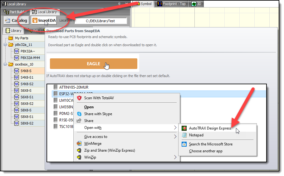
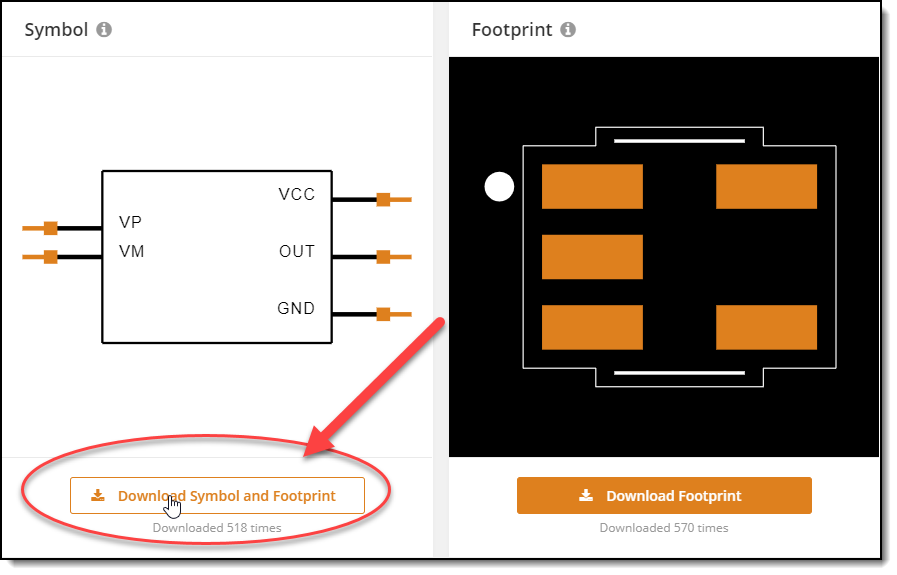
Download File Type
Download both the Symbol and Footprint.
Click on Eagle for the download file type.

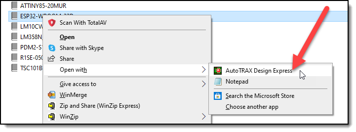
Opening the Part
Once downloaded you can open the part by double clicking on it.
If DEX does not startup the you can set the default app for the file type by right clicking on the file.
Sunday 1 January, 2023
![]() Part References
Part References
Fix for changes to part references in symbols and footprints not updating the 3D view.
SnapEDA Part Imports
Improved symbols for SnapEDA parts.