Whats New for 2024
December
Tuesday 31 December 2024
Polygon Shapes
You can now set the start and end caps for polylines.
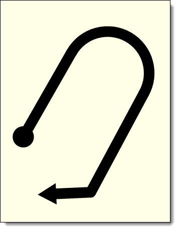
Polyline Start and End Cap
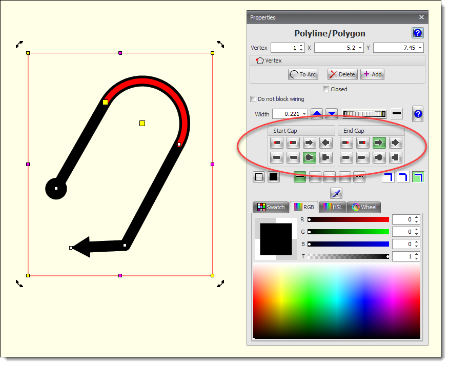
Setting Polyline Start and End Caps
Monday 30 December 2024
Polygon Shapes
New polygon shapes. NOTE: User interface keys changed. See below. This makes it a lot simpler.
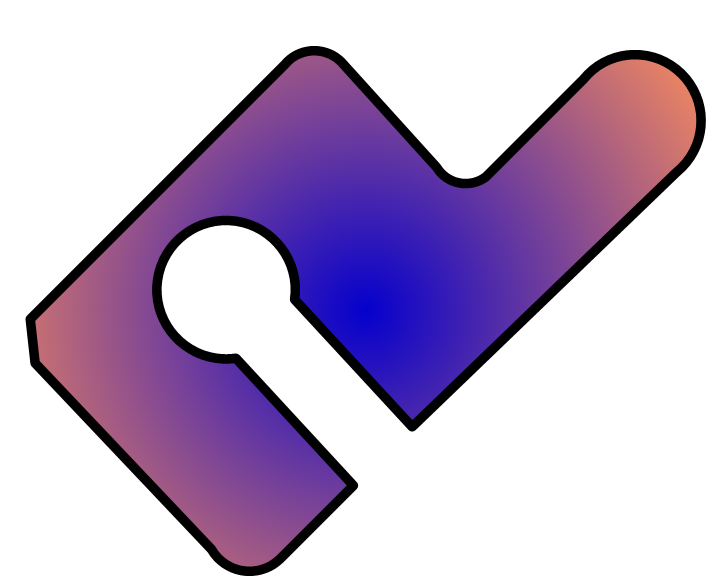
Typical Polygon Shape
NOTE:
•Polygonal copper pours
•Polygonal split power planes
•Polygonal keepouts
•Polygonal cutouts
•Polygonal no masks
•Polygonal pads
•Polygonal PCB border
•Polygonal holes
all work the same.
The shapes are very easy to create and very powerful. Far easier than Bézier shapes. Once created, they can be converted to Bézier shapes.
Adding Polygons:
Click on Add->Graphical Shapes

Add Open or Closed Polygon
While adding: NOTE: User interface keys changed.
•Normally straight edges are added.
•Left Click to start adding the first or another or the first polygon line segment.
•Press the 'S' key to toggle the snap to grid.
•Press the Shift to toggle the current segment between an arc and a straight line.
•Pressing the Tab key to reverse direction of the arc.
•Press the 'O' or 'C' key to toggle between an open and a closed polygon.
•Press the Esc or Backspace key to undo adding the last segment. This removes the last segment.
•Press the End key or Double Left Click to end adding the polygon.
Practice makes perfect.
Editing Polygon
•Select the polygon/polyline
•Press the Shift to toggle the selected segment between an arc and a straight line.
•Press the Tab key to reverse direction of the selected segment's arc (if it is an arc).
•Press the 'O' or 'C' key to toggle the selected segment between an open and the closed polygon.
•Press the 'O' or 'C' key to toggle the selected segment between an open and the closed polygon.
•Press '-' key to delete the selected vertex.
•Press Del to delete the polygon.
•Press '+' key to add a vertex.
•Double click on any line/arc segment to add a vertex.
•Drag an edge to move it.
•Drag a vertex to move it.
•Use the properties panel. Press F2 to toggle the visibility of the Popup Properties Panel. You can set colors, line width and style, corner styles.
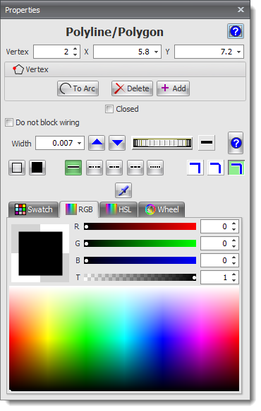
THe Polyline/Polygon Properties Editor
Saturday 28 December 2024
Polygon Shapes
New polygon shapes.
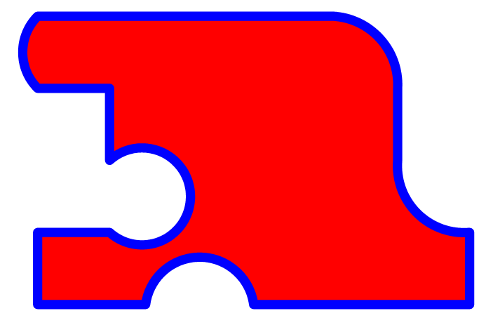
Typical Polygon Shape
NOTE:
•Polygonal copper pours
•Polygonal split power planes
•Polygonal keepouts
•Polygonal cutouts
•Polygonal no masks
•Polygonal pads
•Polygonal PCB border
•Polygonal holes
all work the same.
The shapes are very easy to create and very powerful. Far easier than Bézier shapes. Once created, they can be converted to Bézier shapes.
How To:
Click on Add->Graphical Shapes

Add Open or Closed Polygon
While adding:
•Normally straight edges are added.
•Press 'C' to start an arc.
•Pressing 'Tab' or 'Space' key to reverse direction of the arc.
•Press the 'L' key to revert to a straight line.
Practice makes perfect.
Thursday 26 December 2024
Effective June 7, 2026, Autodesk will no longer sell nor support EAGLE.
Autodesk recommend you to subscribe to Autodesk Fusion for access to the electronics workspace - In other words your designs!
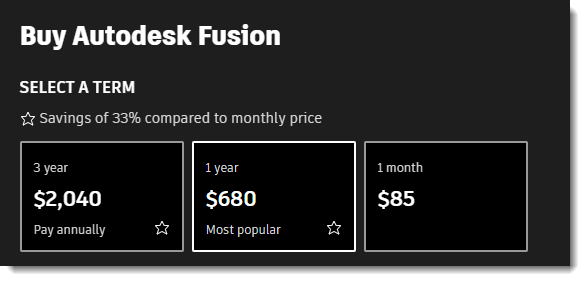
Rental Prices for Autodesk Fusion.
You NEVER own it.
Autodesk Eagle Project Import
Improved import of text. Some were not placed correctly.
PCB borders, curved edge.
Command line opening of Eagle schematics and boards (both merged into one AutoTRAX DEX project). This allows double clicking on Eagle brd and sch files to open them in AutoTRAX DEX.
Thursday 19 December 2024
 Bug Fix
 Rotate 90° clockwise/anti-clockwise was reversed.
Tuesday 17 December 2024
 Bug Fixes
•Fix for Gerber solder mask layers having teardrops on pads if teardrops enabled.
•Fix for the Gerber viewer showing tracks with flat (not rounded) corners.
Thursday 12 December 2024
Desktop Icons Updated
New'ish' Splashscreen

New Splashscreen
Wednesday 11 December 2024
AutoTRAX DEX PCB Designer changed to AutoTRAX DEX PCB Designer
This keeps it simpler and using AutoTRAX DEX for the short name keeps the program name simpler and more human.
AutoTRAX DEX PCB Designer Installation
New Directories
C:\ProgramData\AutoTRAX Software now uses C:\ProgramData\AutoTRAX DEX PCB Software
C:\Users\XXX\AppData\Local\AutoTRAX Software now uses C:\Users\XXX\AppData\Local\AutoTRAX DEX PCB Software
C:\Users\XXX\AppData\Roaming\AutoTRAX Software now uses C:\Users\XXX\AppData\Roaming\AutoTRAX DEX PCB Software
Where XXX is you.
The old directories are not deleted. AutoTRAX DEX copies the old contents to the new directories.
You can keep or delete the old AutoTRAX program.
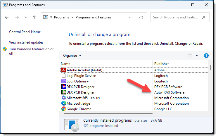
Uninstall Old Version
Desktop Icon Changed to AutoTRAX DEX
Desktop Icon
Tuesday 10 December 2024
Simulation Instruments
Opening new project updates the Spice Analysis.
Improved instruments.
Friday 6 December 2024
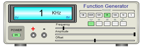
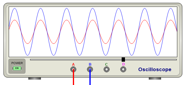
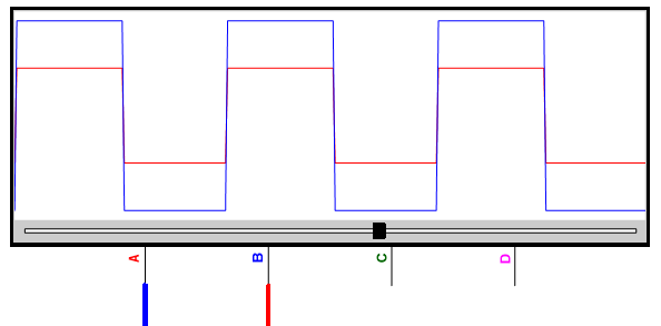
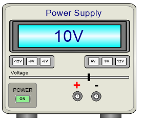
Simulation Instruments
Improved instruments.
Monday 2 December 2024
Simulation Chart/Oscilloscope
Added time and voltage labels.
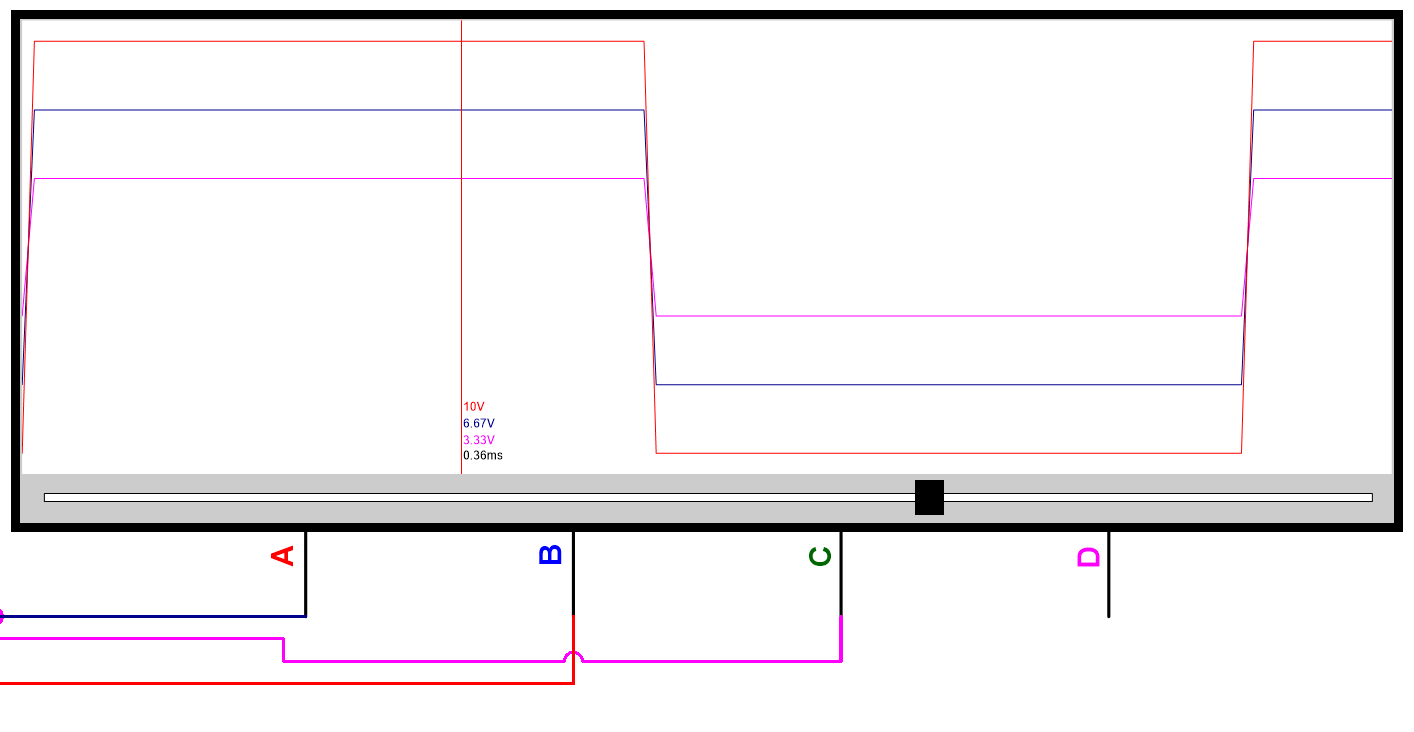
Chart with Labels
Sunday 1 December 2024
Bluesky
Social media as it should be. Find your community among millions of users, unleash your creativity, and have some fun again. Follow the AutoTRAX DEX PCB Designer news.
https://bsky.app/profile/pcbdesign.bsky.social
https://bsky.app/profile/autotrax.bsky.social
Simulation Instruments
Editors for the Function Generator and the Power Supply
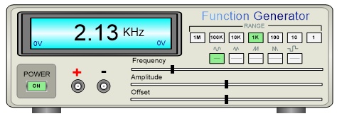 A Function Generator |
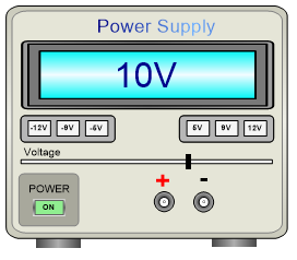 A Power Supply |
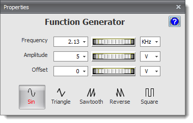 The Function Generator Properties Editor |
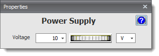 The Power Supply Properties Editor |
November
Sunday 24 November 2024
 Minor Bug Fixes
•Improved Samples
•Fix for text size of footprint part values
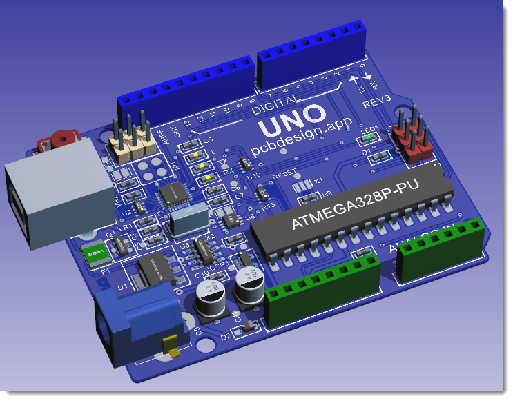
Fix for Text Size of Footprint Part Values
Monday 18 November 2024
Plotting
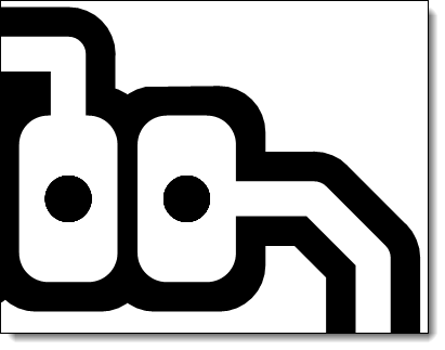
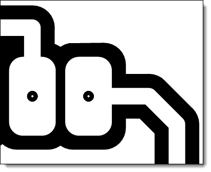
•You can show/hide the holes.
•You can show/hide the pilot holes.
Both of the above act independently.
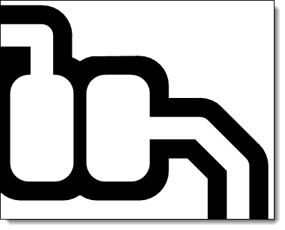 No Hole or Pilot Hole |
 Holes |
 Drill Pilot Hole |
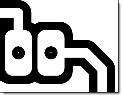 Hole and Drill Pilot Hole |
Sunday 10 November 2024
Plot
You can now array the plots.
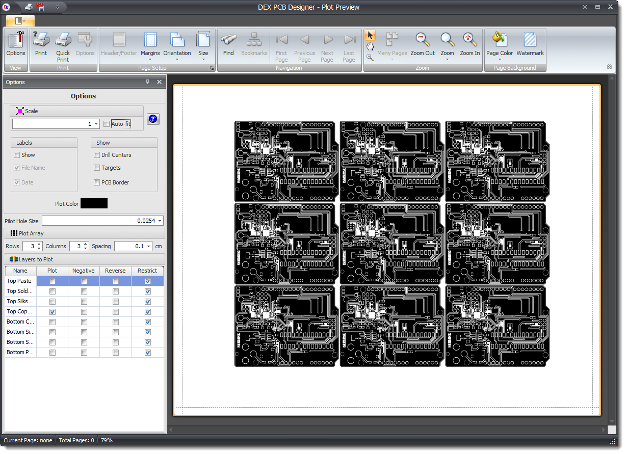
Plot Array
Saturday 9 November 2024
Copper Pour
 Fix for removal of non-connected copper pour regions.
Tuesday 5 November 2024
DRC
The DRC flags cutouts overlapping the PCB Border. Change the PCB Border shape instead to save manufacturing costs.
Friday 1 November 2024
Improved Shortcuts Editor
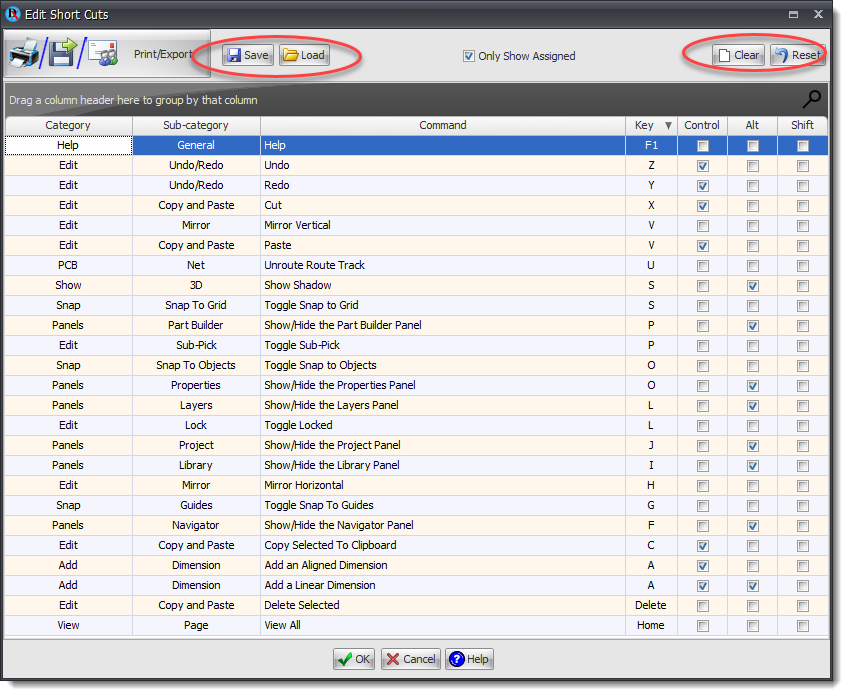
Improved Shortcuts Editor
October
Thursday 31 October 2024
Improved PCB Stack Editor
Added thumb-wheels for adjusting the PCB thickness.
 Fixed some thickness calculation errors for single-sided PCBs.
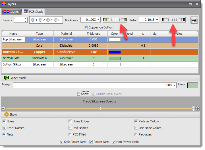
Improved PCB Stack Editor
You can now:
•Reset
•Clear
•Save
•Load
Wednesday 30 October 2024
 Fix for STL Output
PCB board was not output.
 Fix PCB Layer Stack
Incorrect thickness calculations for single side PCBs.
Monday 28 October 2024
Improved Shortcuts Editor
Duplicates highlighted.
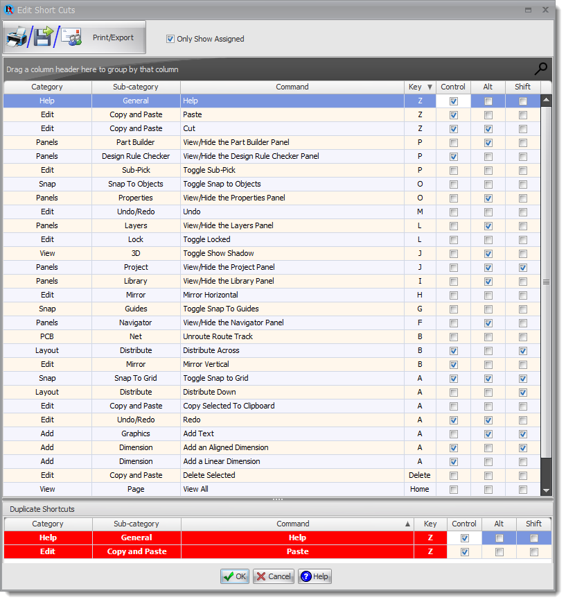
Improved Shortcuts Editor
Sunday 27 October 2024
Adding SMT Parts to Single Sided PCBs
Automatically set sides to the side with the copper.
 Various User Interface Fixes and Improvement
Friday 25 October 2024
New Design States Control in the Project Panel
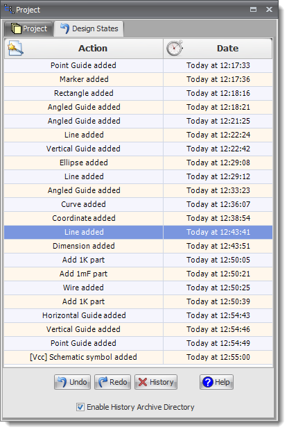
Design States
New Popup Design States Manager
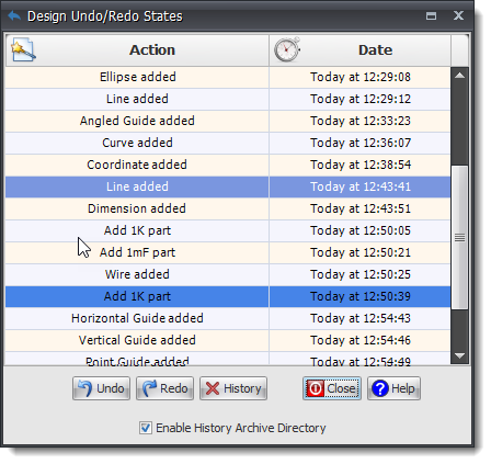
Popup Design States Manager
New Recover Dialog
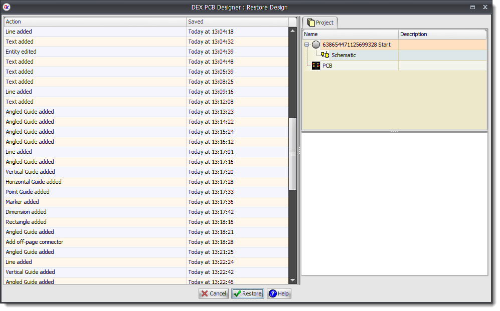
Recover Dialog
Tuesday 22 October 2024
Optimization
Removed excess updates of controls after changes.
 Fix for the Some Controls Losing Focus After Entering Text.
Monday 21 October 2024
Project Panel - Now has a Undo/Redo Manager
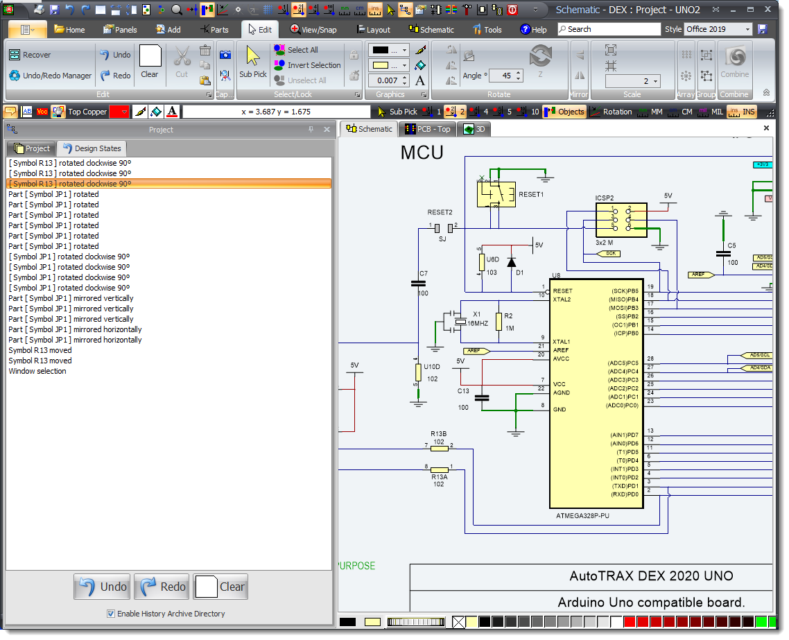
Project Panel - Undo/Redo Manager
Rotate
If multiple items are selected, then they are rotated about their combined center. not all objects can be rotated in a collection.
Mirror
If multiple items are selected, then they are mirrored about their combined center.
Sunday 20 October 2024
 Fix for the ColorBar bottom-clipping panels docked on the right.
Saturday 19 October 2024
Improve Clipping
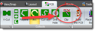
Clipping
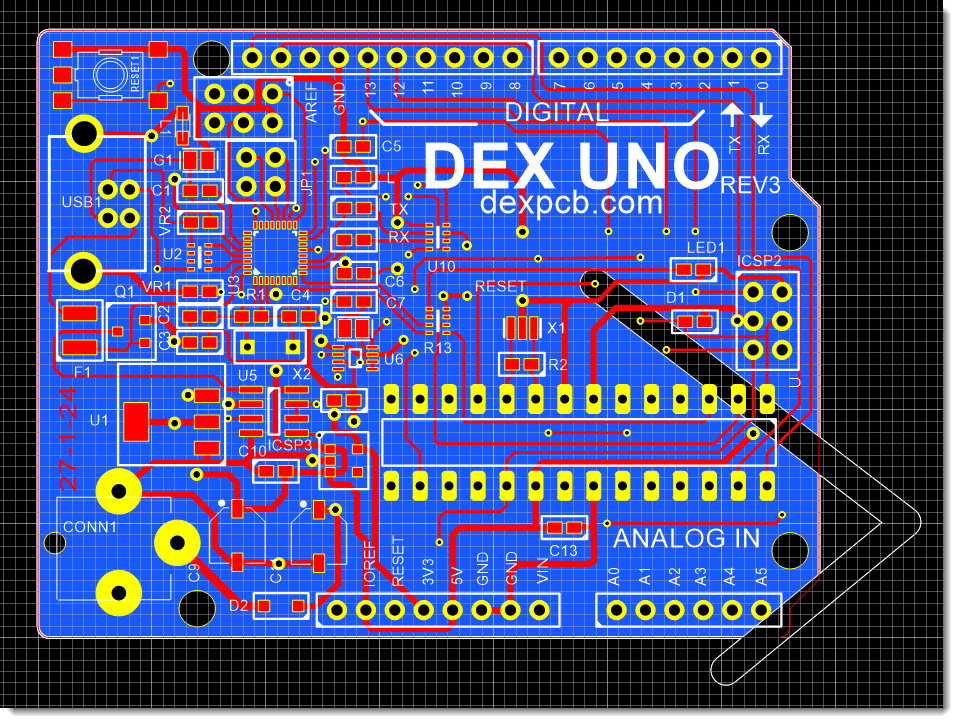
Not Clipped
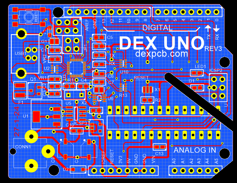
Clipped
Improved Add Polyline/Polygon/Keep-out/PCB Borders,No Mask, Copper Pour etc.
Friday 18 October 2024
Select After Create
After objects added, they are set as selected. This works well with the Popup Properties Panel and allows you to edit objects immediately after creation.
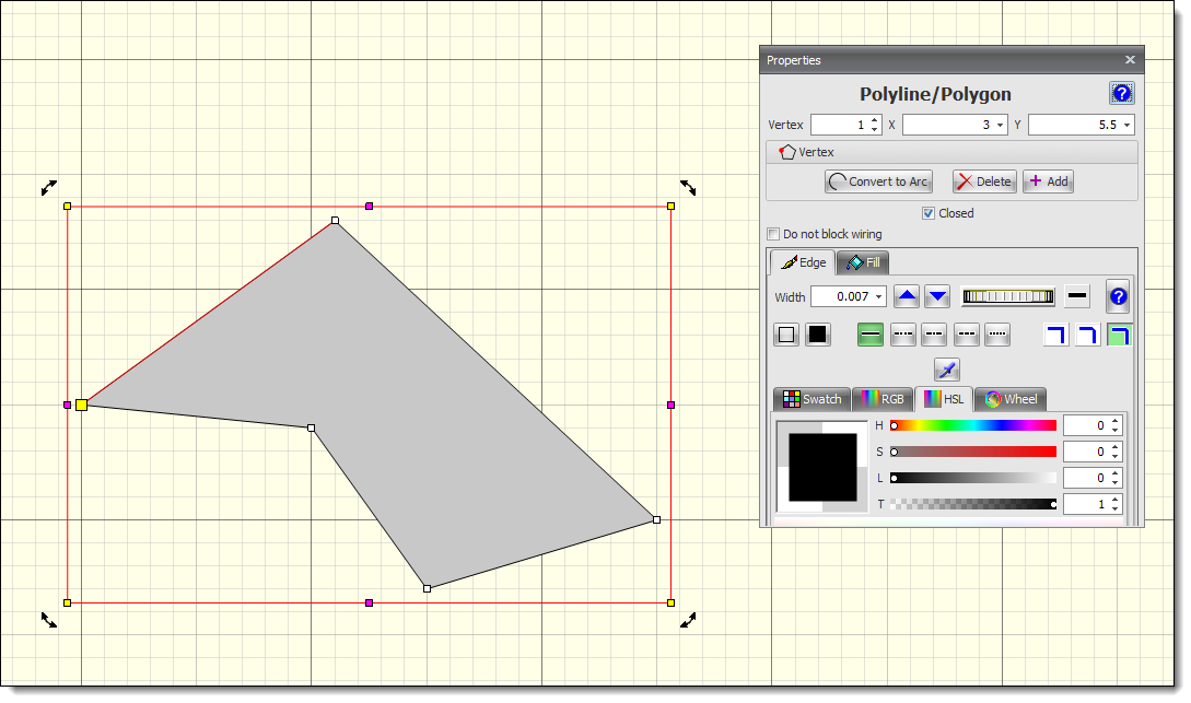 After Polygon Addition - Selected With Popup Properties Editor |
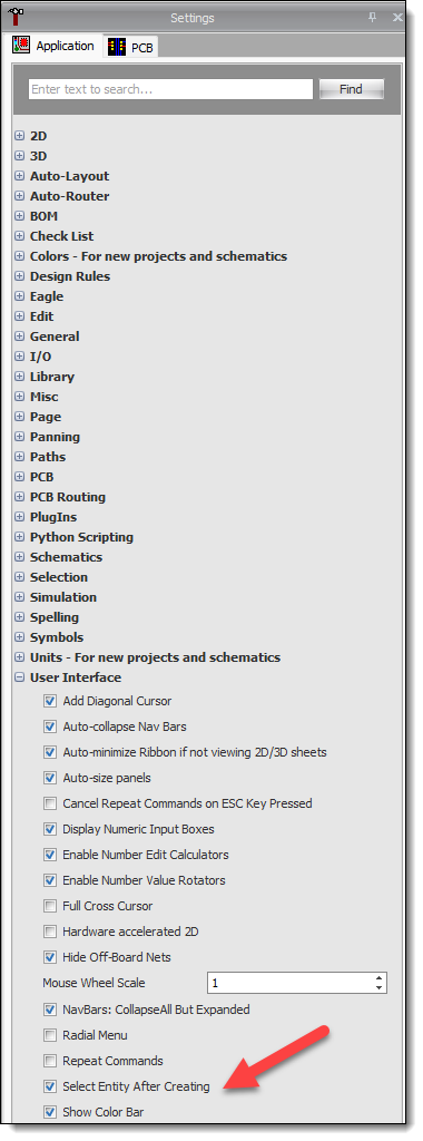 Enable/Disable Select After Create |
Bug Fix
 Fix for arc shaped PCB cutouts appearing white not transparent.
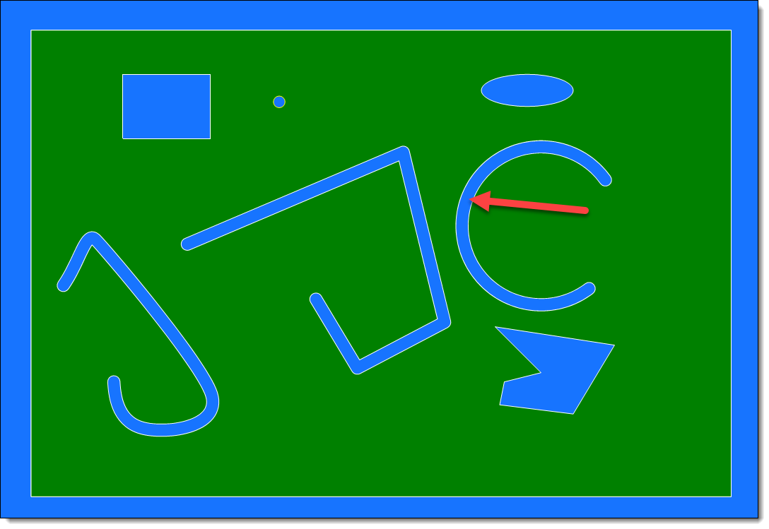
PCB Cutouts With Blue Background
 Wednesday 16 October 2024
Bug Fix
•Fix for 3D view of single layer PCB's.
 Tuesday 15 October 2024
Bug Fixes
•Error for vias not connected to tracks.
•Quad solder error.
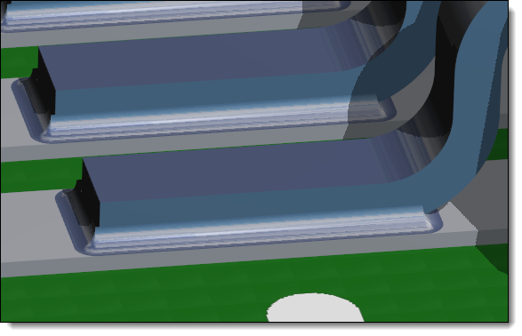
Quad Solder Error Fixed
Monday 14 October 2024
Help Website
•Improved context sensitive links to the online help.
Sunday 13 October 2024
Help Website (This)
•Improved help.
•Better links from AutoTRAX DEX.
Monday 7 October 2024
File Names
Prevention of illegal file names.
Sunday 6 October 2024
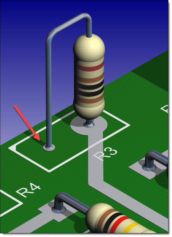
 Auto-minimize Pad
Fixed bugs.
Friday 4 October 2024
Design States
 Fixed some states not being set.
All design states now have a more descriptive label.
Thursday 3 October 2024
History Directory
The History directory has more descriptive labels for the design states.
Every change you make to a design is saved in the .History directory for a project/part. The design state files are never deleted by AutoTRAX DEX. This provides an 'audit trail' for your designs.
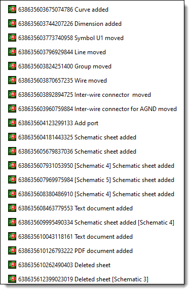
Sample History Directory
Added Design States Tab
New Design States tab in the Projects Panel.
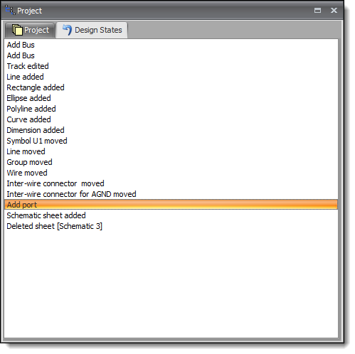
Design States
Wednesday 2 October 2024
 Fixed internal bugs and self repair.
Tuesday 1 October 2024
Add/Remove Copper pour margin to PCB
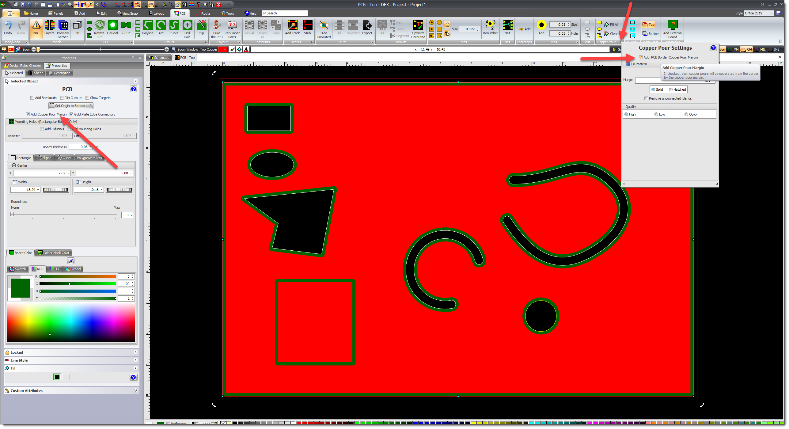
Add/Remove Copper pour to PCB margin
 Fix parametric two-sided footprint pad count change not immediately reflected in other controls.
 Fix for part value sometimes being cleared.
September
Saturday 28 September 2024
 Fixed copper pour sometimes not connecting to pads.
 Fix for numeric entry sometimes not working.
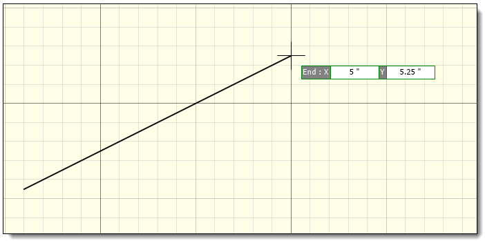
Numeric Input for Line End
Wednesday 25 September 2024
•Zoom Window works correctly in Paneled PCB views.
•V-Cuts now displayed in 3D Views (Non-Paneled PCBs)
•Diagonal cross hatch pattern for PCB panels.
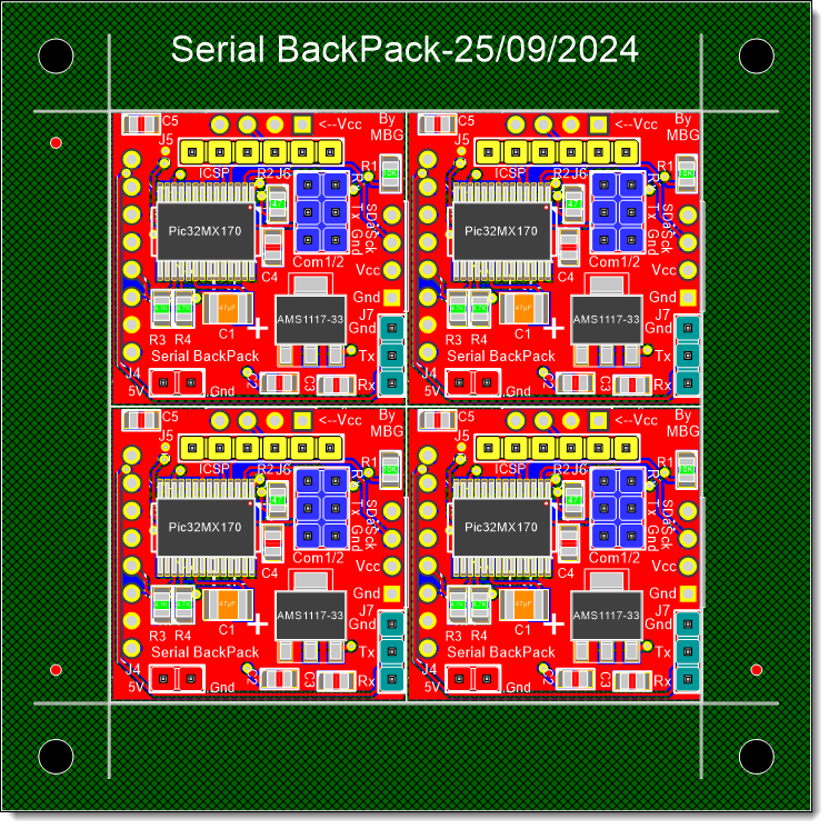
Panel Hatching
Sunday 22 September 2024
Learn about general features that apply to all area of PCB design.
In these videos you will learn how to use the AutoTRAX DEX PCB Designer interface to get the most productive environment. Videos include full screen, viewports, floating end docking control panels and of course the menus.
These videos show you how to create electronic parts for your schematics. You will learn about both custom and parametric parts.
You will learn how to create schematics for your PCB designs. Topics include adding parts, editing parts, connecting parts together, and auto-routing of this schematic wires.
Do you want to have fun simulating the analogue behaviour of your PCB's? Then these videos are just what you are looking for.
Learn how to create your PCB's. Topics include placing end orientating footprints, manually routing the PCB tracks, the all-important design rule checker, copper pours, keep out regions and PCB panelization.
With the AutoTRAX DEX PCB Designer you can add stunning and beautiful graphical items to your symbols, schematics and even your PCB's. These videos show you how.
Do you want to see what your PCB will really look like before you have it manufactured? These videos will show you how to view your PCB in glorious 3D.
Download All Videos
You can now download all the tutorial videos..
Sunday 15 September 2024
Sunday 8 September 2024
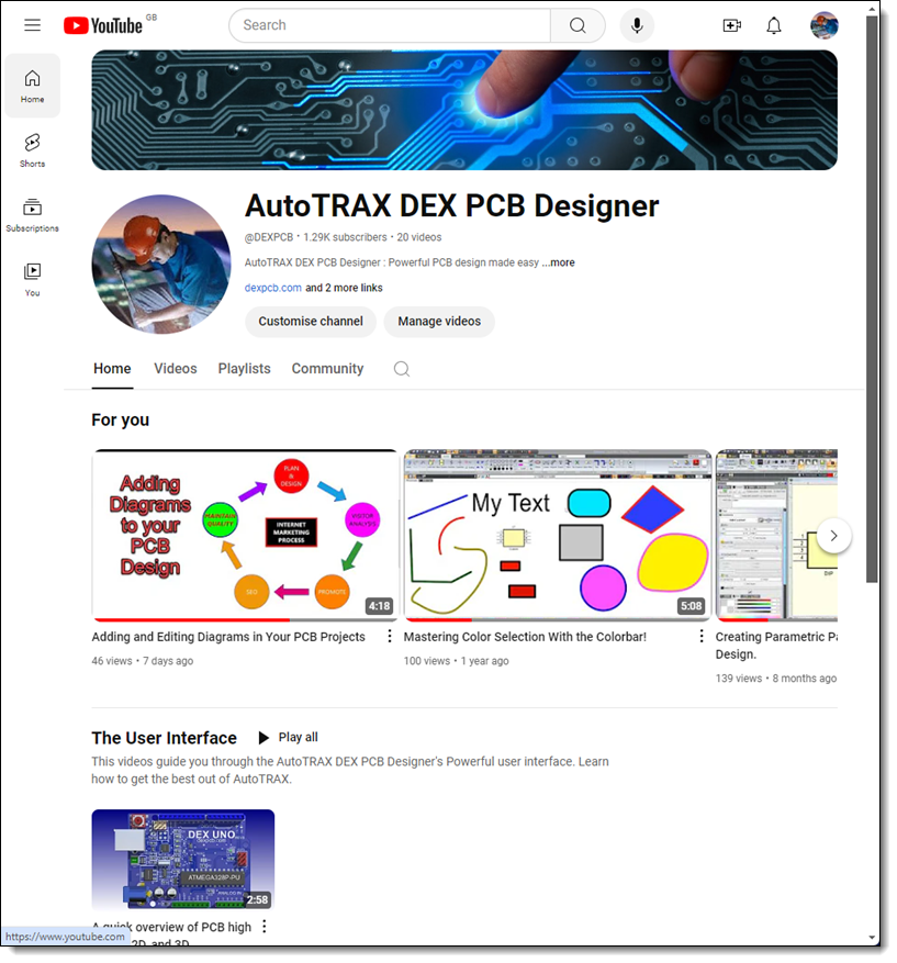
YouTube Videos
Many old and out of date videos removed. These will be replaced in the coming days by improved videos. View...
YouTube
Sunday 1 September 2024
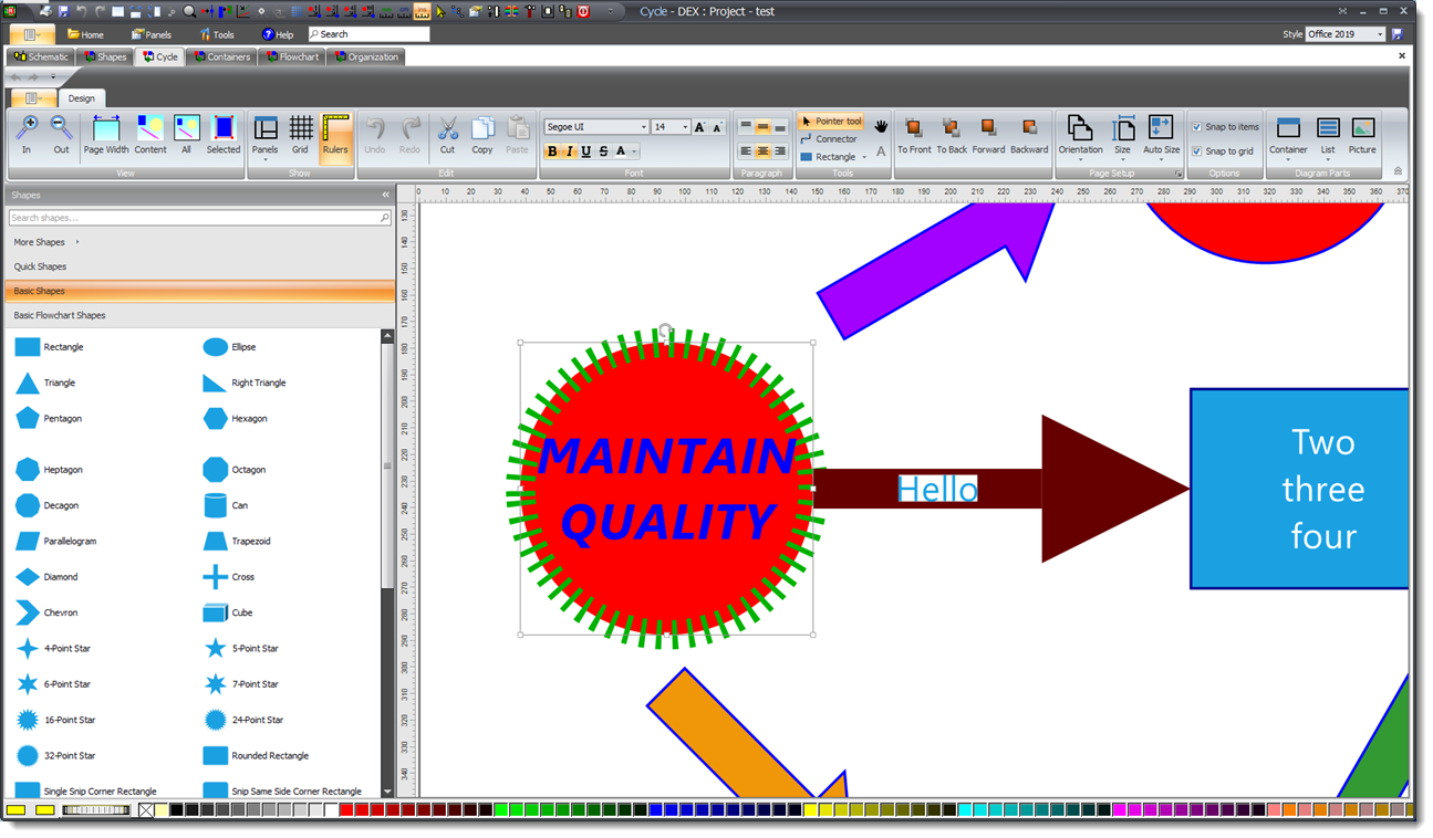
Diagram Sheets
Optimized diagram viewport and panels.
Diagrams
August
Monday 26 August 2024
Diagram Sheets
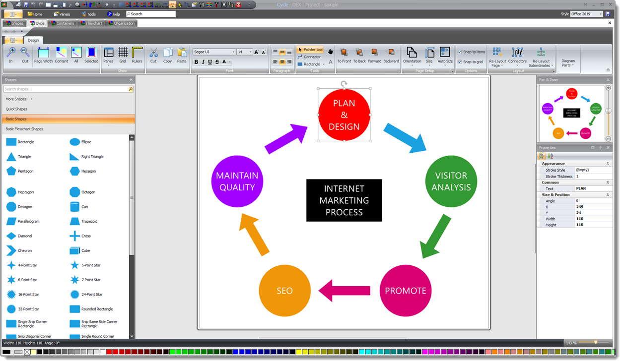
You can now add diagram sheets to your designs.

Add Diagram Sheet

Sample Diagrams Project
Sample Diagrams Project
Thursday 15 August 2024
New PolyShapes

Add PolyShape Button
Similar to polylines except some edges can be arcs. Press 'A' key for arc segment.
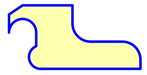
Closed PolyShape
PolyShapes, Arcs, Polygons and Curves
PolyShapes, Arcs, Polygons and Curves can be filled even if not closed.
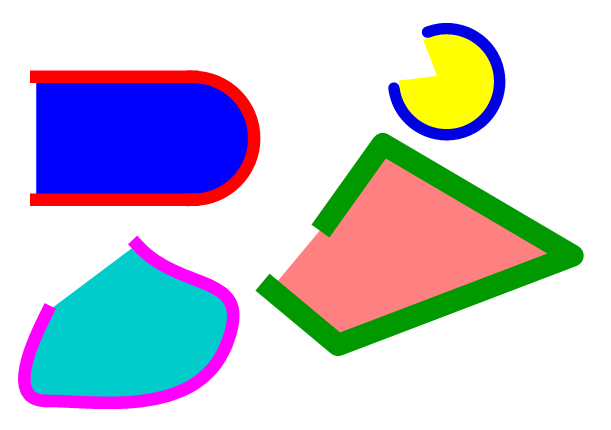
Open Shapes with Fill
July
Monday 22 July 2024
KiCad Parts
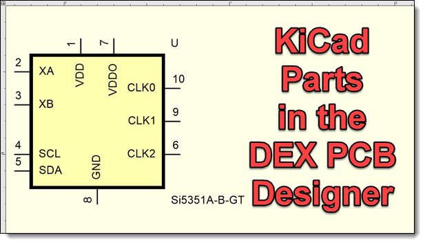
KiCad Parametric Parts
AutoTRAX DEX now comes with approximately four thousand KiCad free community parts. They have been pre-converted for you and each schematic, and footprint that are separate in KiCad have been combined into a single parametric part.
There are plans to add many more of the parts provided by the KiCad community.
The converted parts index In AutoTRAX DEX are also free and you are free to distribute, and/ or modify them.
The symbols are easily edited.
Every parametric part also comes with the automatically generated 3D model so there is no need to import inflexible models provided by third parties. Being parametric, the 3D model is automatically generated based on the parameters of the footprint. So, if you change the pad shapes or pad sizes, the 3D model is automatically updated.
If you change the pitch of the footprint pads, then again, the 3D model is automatically updated in real-time. This makes your life far easier, and it makes the file sizes far smaller as no 3D model data needs to be saved.
Thursday 18 July 2024
The Parts Catalog
The Parts Catalog now has 58,215 parts
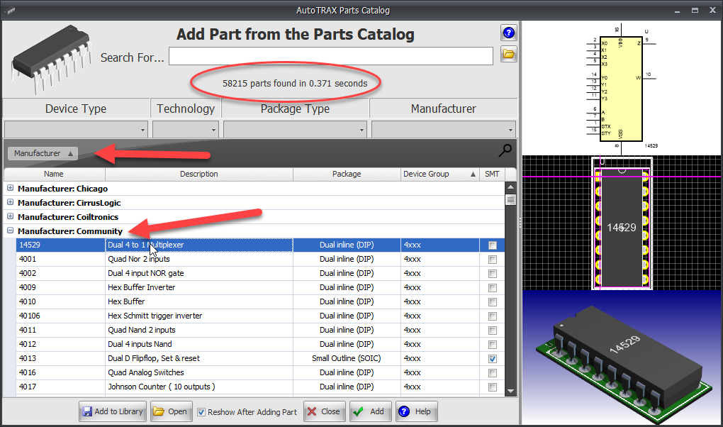
Community Parts
KiCad Community Free Parts
Available in the Library panel and the Parts Catalog.
Note: You will need the latest version to view the parts correctly.
.
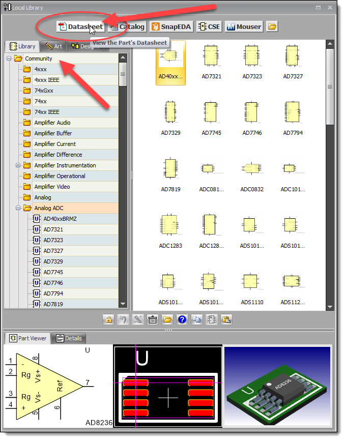
KiCad Community Free PartsKiCad Community Free Parts
Thursday 18 July 2024
KiCad Import
Internal changes to handle the 'oddities' of KiCad graphics: imported parts.
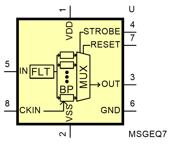
Imported KiCad Part
Friday 12 July 2024
Snap to Objects
Snap to objects now shows a circle to confirm snap.
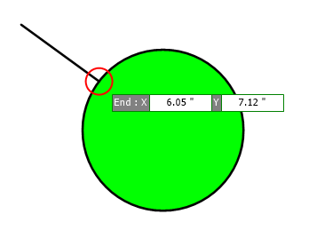
Snap to Objects
Adding Arcs
Three add arc commands.
NOTE: During creation, pressing the TAB key reverses the arc start and end angles.
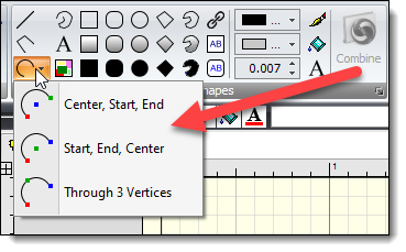
Add Arc Commands
Friday 5 July 2024
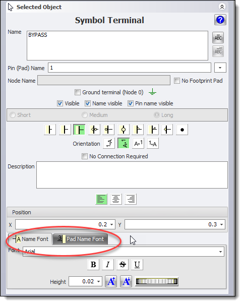
Symbol Terminal Fonts
Separate Font for Symbol Terminal Names and Pad Names
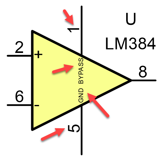
Symbol Terminal Fonts
June
Sunday 30 June 2024
Part Catalog Dialog
Improved layout.
 Fixed bug that could cause the download of the latest catalog to fail.
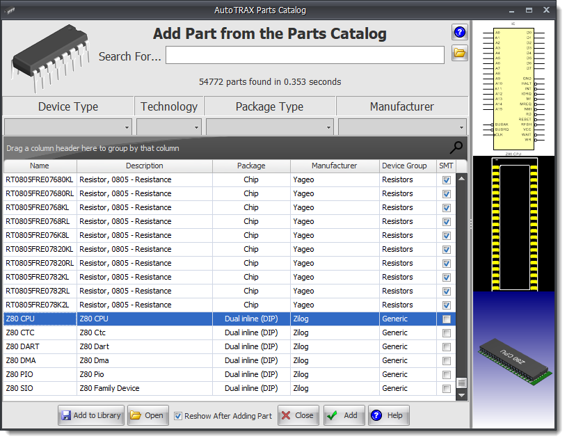
Part Catalog Dialog
Friday 21 June 2024
Simulation Disabled by Default
This makes the user interface slightly simpler.
See Settings->Simulation->Enable Simulation.
Thursday 20 June 2024
Improved Route Panel With New Buttons
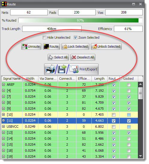
Route Panel
Wednesday 19 June 2024
How to Build a PCB in Only 23 Seconds
This videos show you how to build a PCB on only 23 seconds. The actual time depends on the performance of the company.
How to Build an Arduino Compatible PCB in a Stunning 23 Seconds

Monday 17 June 2024
Locked PCB Nets
Locked PCB Nets cannot be unrouted.
Locked PCB Nets in the Route Panel
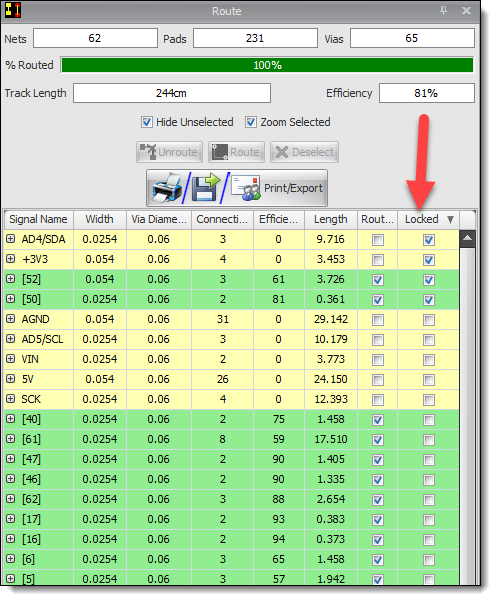
Locked PCB Nets in the Route Panel
Monday 10 June 2024
Locked Objects
If the following objects are locked then all sub-objects owned by the object are also locked.
•Groups - all contained entities.
•Footprints - pads, value, reference, graphics etc
•Symbols - terminals, value reference, graphics etc.
•PCB Border - cutouts and drill holes.
•PCB Nets - tracks, vias, track junctions.
Thursday 6 June 2024
Gerber Output
Added additional optional Gerber output file for profile and cutouts.
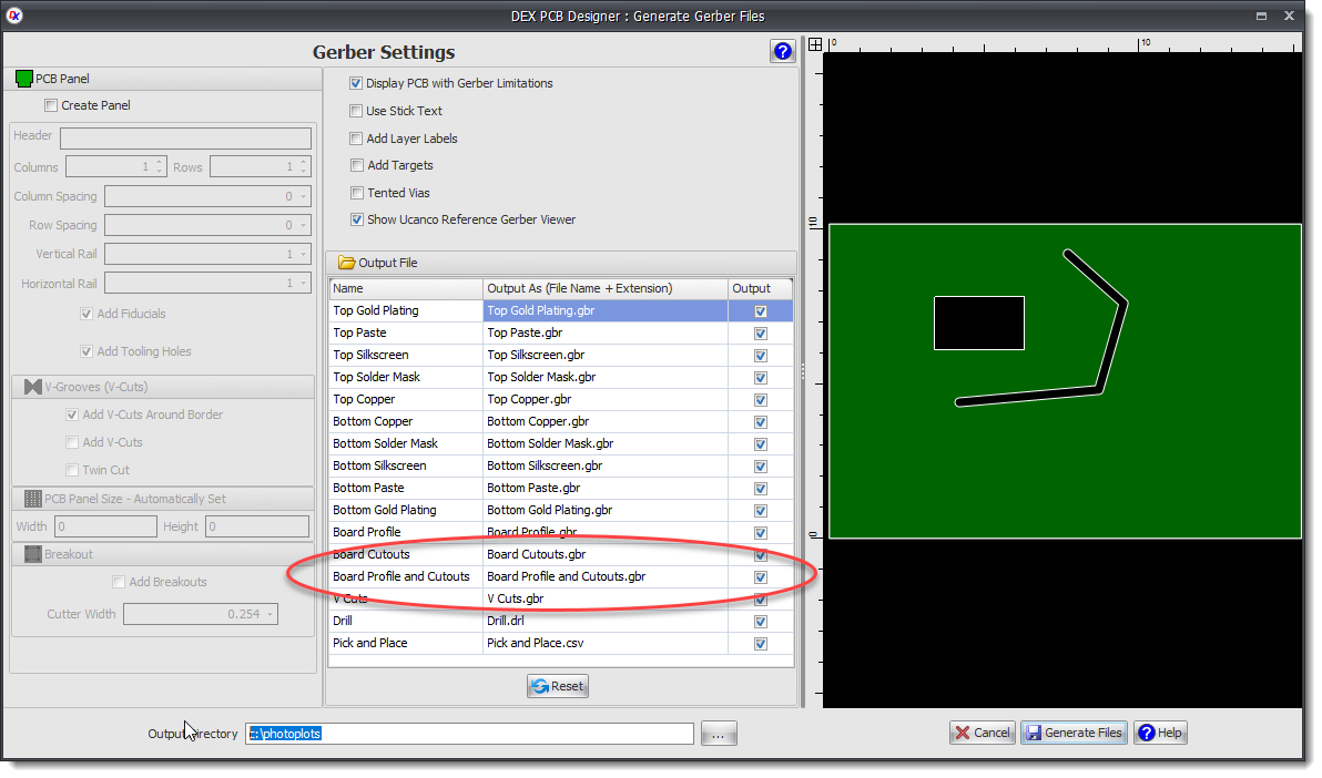
Profile and Cutouts
Wednesday 5 June 2024
Spreadsheets
You can now add spreadsheets to you design.

Addding a Spreadsheet to Your Design
User Interface
If you are viewing a non 2D/3D sheet then the main ribbon menu is automatically minimized. It is expand if a 2D/3D sheet is viewed. This avoids clutter.
You can disable auto-minimization in the Settings Panel.
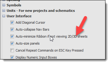
You can disable auto-minimization in the Settings Panel
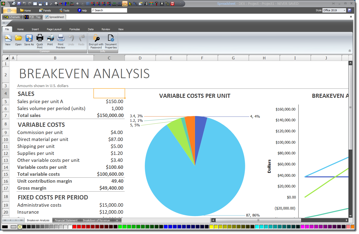
A Spreadsheet Added to a Project
Monday 4 June 2024
Printing Panel Contents
Added Print command buttons to:
•Checklist Panel
•Layers Panel
•Project Panel
•Parts List (BOM) Panel
•Source Panel - Save as XML
•Route Panel
•Short-cuts Editor
Short-cuts Editor
Added Shift Key Pressed Option.
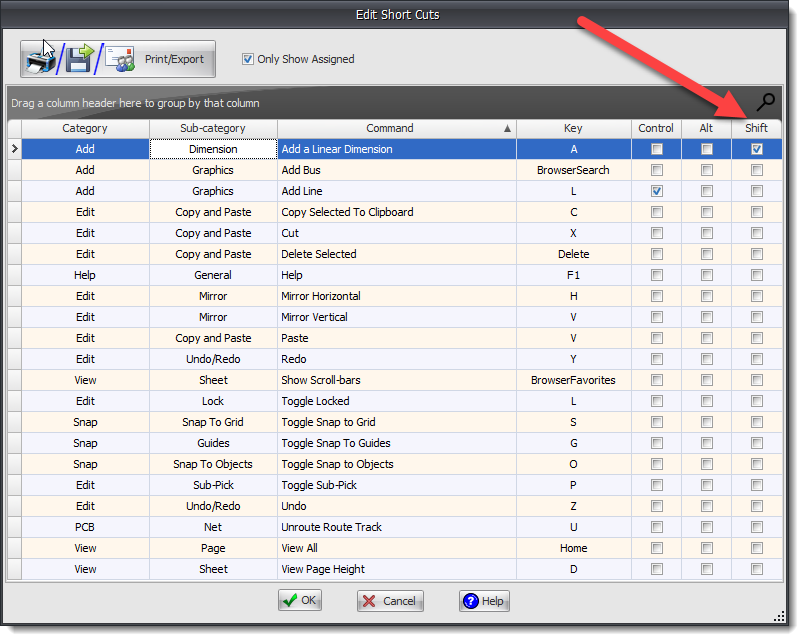
Shift Key Pressed Option
Added print option to print out only assigned shortcuts.
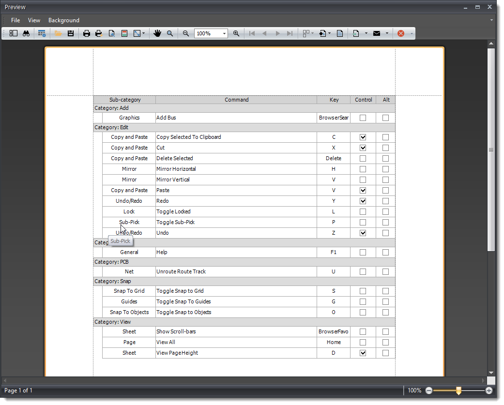
Shortcuts Print Preview
Monday 3 June 2024
Unrouted Tracks
Unrouted tracks now show dotted making them more visible. You have the option to turn off the dotted line style.
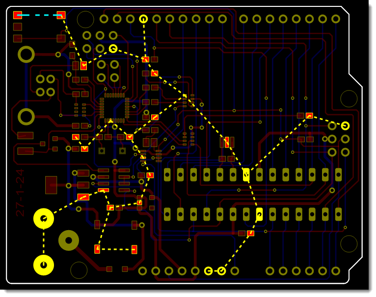
Unrouted Net
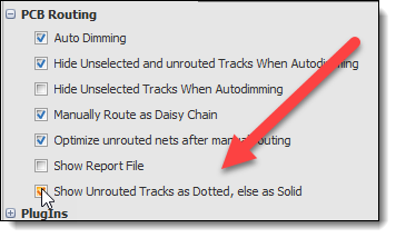
Settings for Dotted Unrouted Tracks
Sunday 2 June 2024
Short-cuts Editor
Added more shortcuts and improved the editor layout.
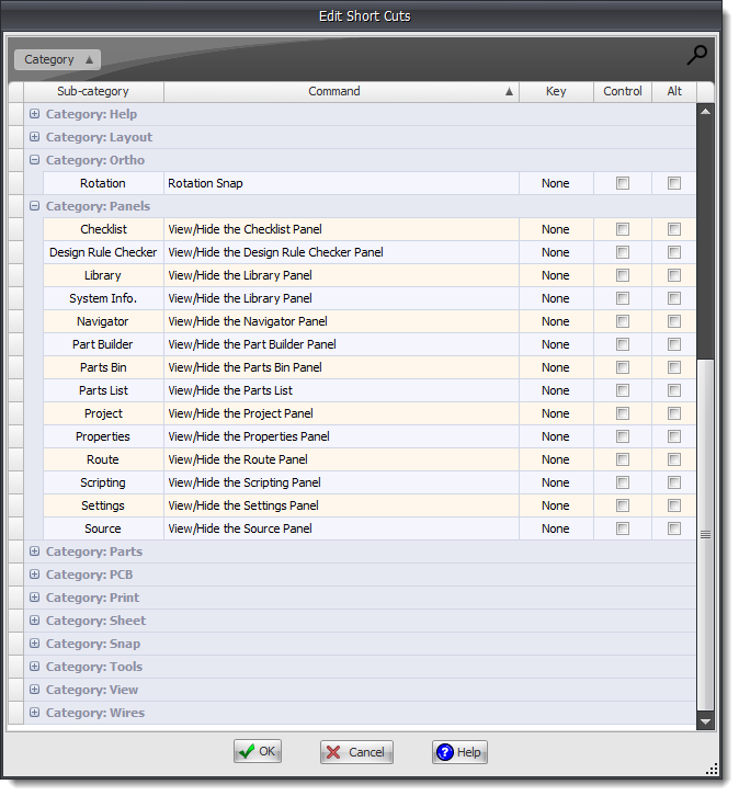
Short-cuts Editor
Saturday 1 June 2024
Shortcuts
Added full list of keyboard keys.
May
Monday 27 May 2024
Op-Amp Sample
Microchip MCP6006 1 MHz Operational Amplifier with EMI Filtering.

Op-Amp Sample
Sunday 26 May 2024
 PCB Copper-pours to Via Gap
Fixed gap size.
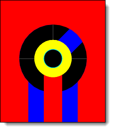
Via to Copper Pour Gap
Settings
Auto-collapse Nav Bars
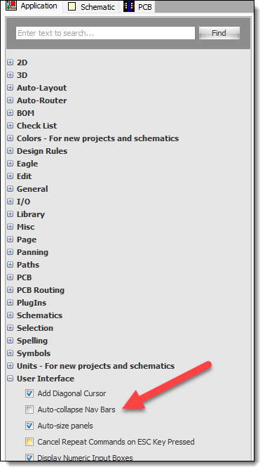
Try uncheck Auto-collapse Nav Bars
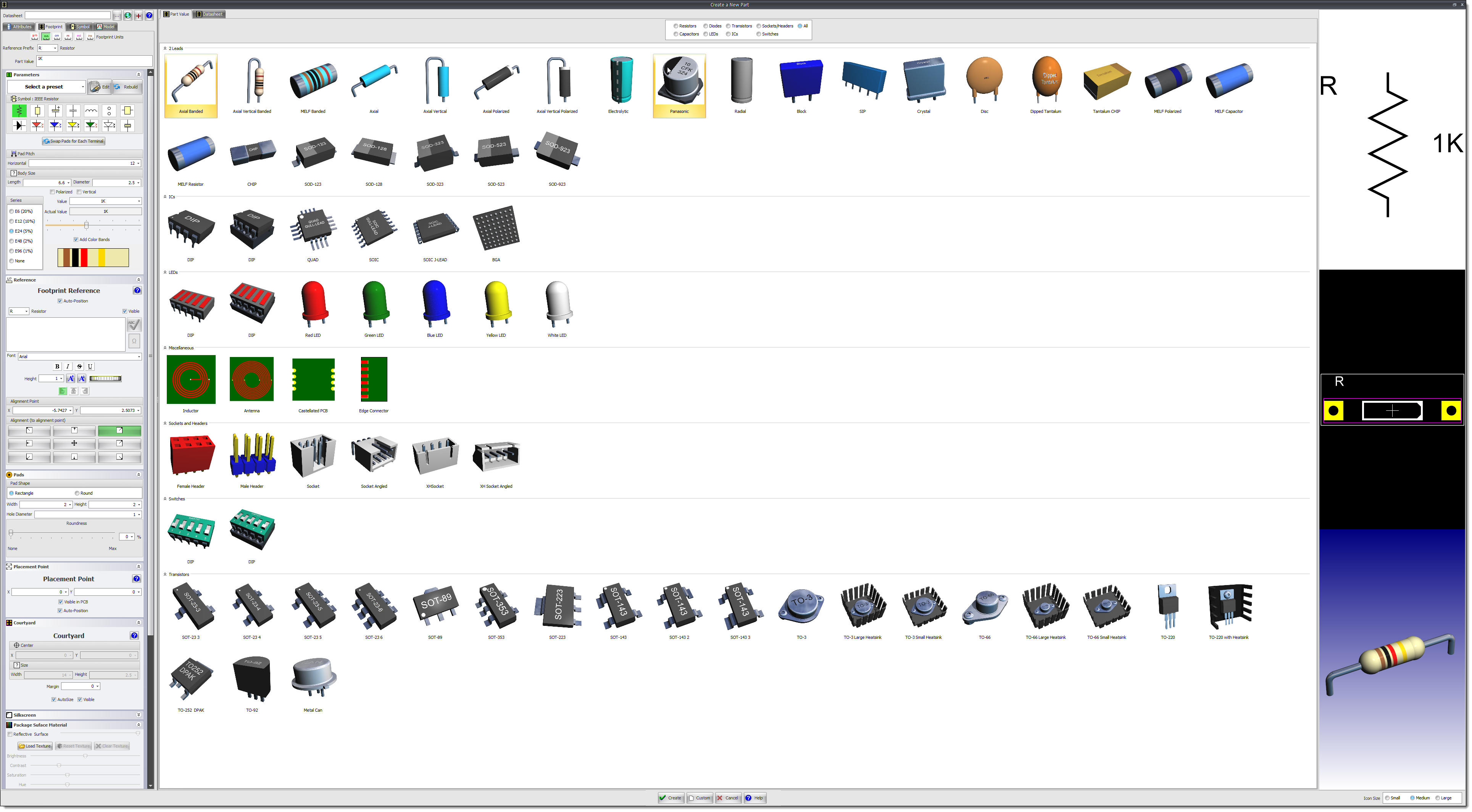
4K Monitor. Text 100% Auto-collapse Nav-Bar off
Saturday 25 May 2024
Symbol Part Types and Footprint Part Types Renamed
Symbol Part Types and Footprint Part Types renamed Symbol Part Values and Footprint Part Values.
Thursday 23 May 2024
Create Part
Improved symbol selection.
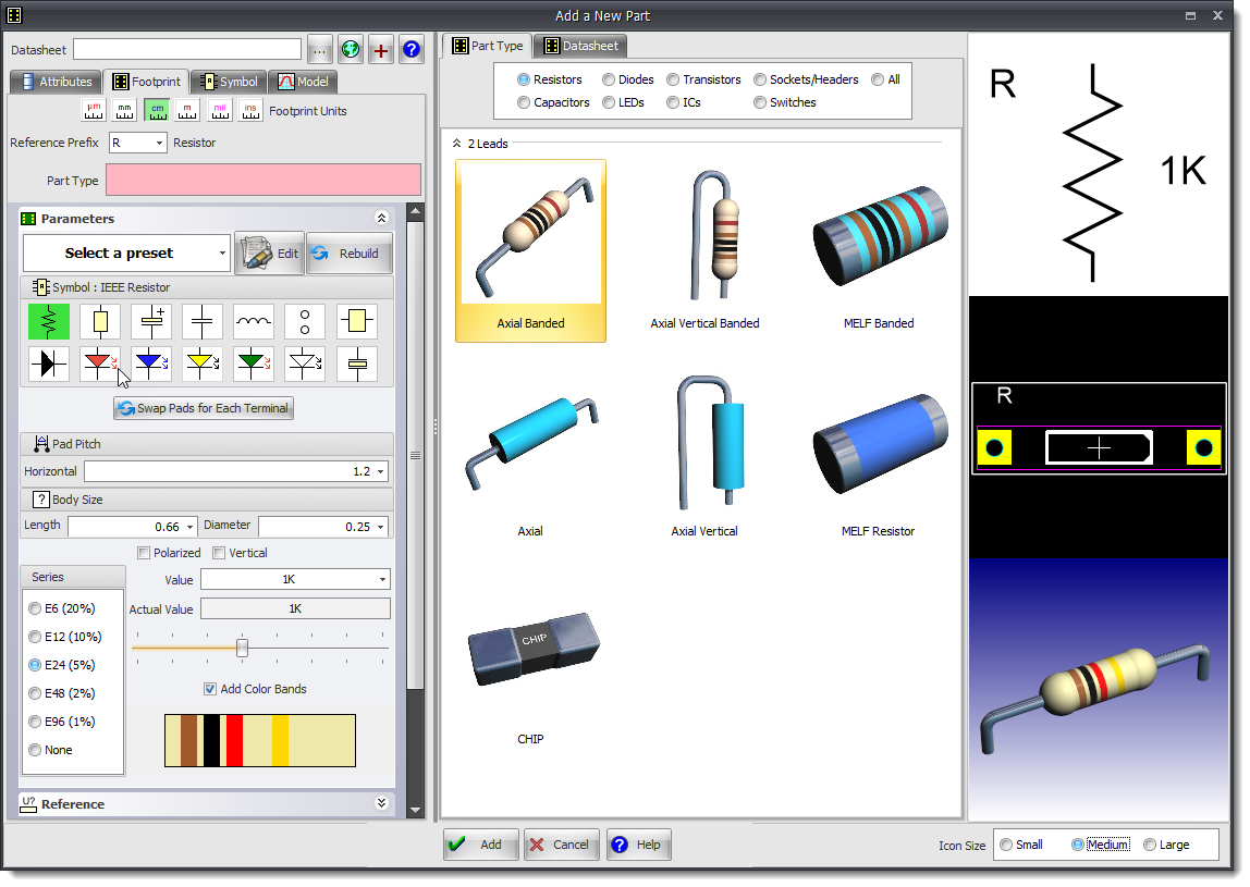
Add a New Part
Wednesday 22 May 2024
 Bug Fixes
 PCB Copper-pours
Fix for removing unconnected copper pour areas failing.
Sunday 19 May 2024
 Bug Fixes
 PCB Copper-pours
Fix some vias not providing correct clearance.
DRC improved.
Friday 17 May 2024
Automatic DIP-style device pins
This is not a parametric part. It is a collection of pads with automatically generated pins, and a rectangle on the top package layer acting as the device body.
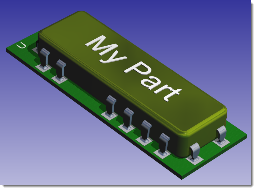
Automatic DIP-style device pins
Thursday 16 May 2024
How to easily create your own custom parts video.
Click to download sample part ...
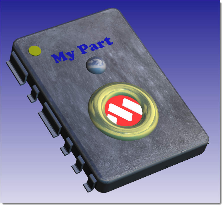
Sample Custom Part
3D Improvements
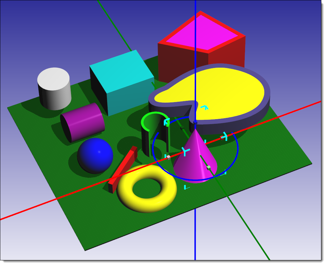
3D Objects
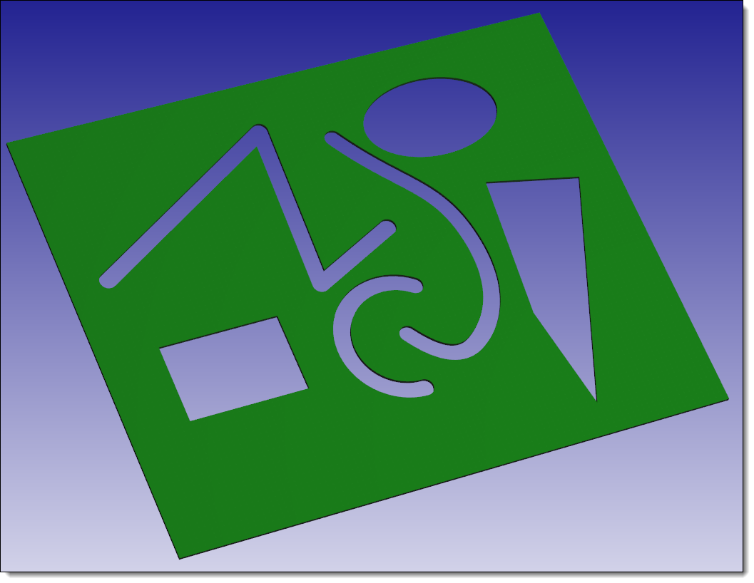
PCB Cutouts
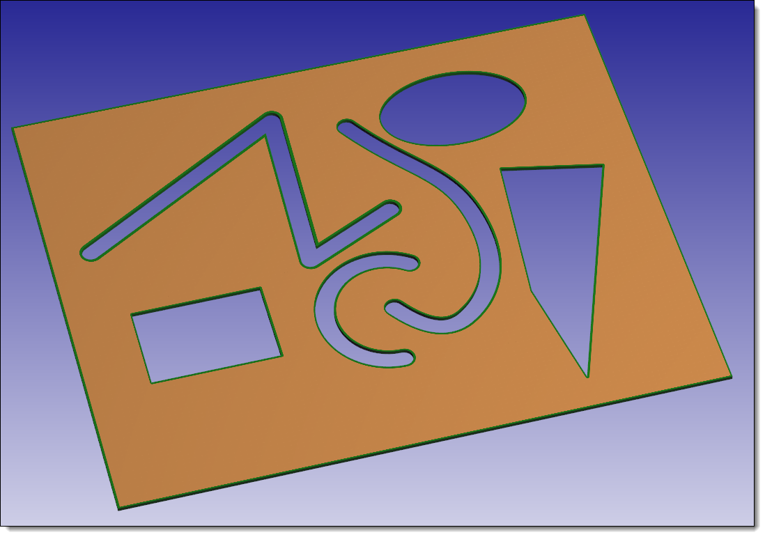
Copper Pours
Wednesday 15 May 2024
 Bug Fixes
 PCB Cutouts
Fix for pcb cutouts not cutting out copper pours correctly if the PCB has been rotated or translated.
•Saturday 11 May 2024
Adding PCB Cutouts
•Adding PCB cutouts clears all copper pours - this stops possible visual confusion and potential design errors.
•Adding PCB cutouts now shows the PCB filled so cutouts show up.
Friday 10 May 2024
Pad Editor
Option to set all pads in footprint.
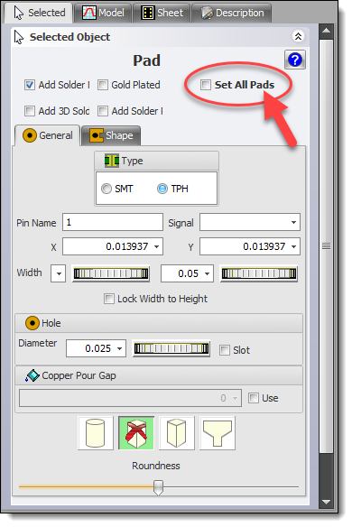
Pad Editor
New Colorbar
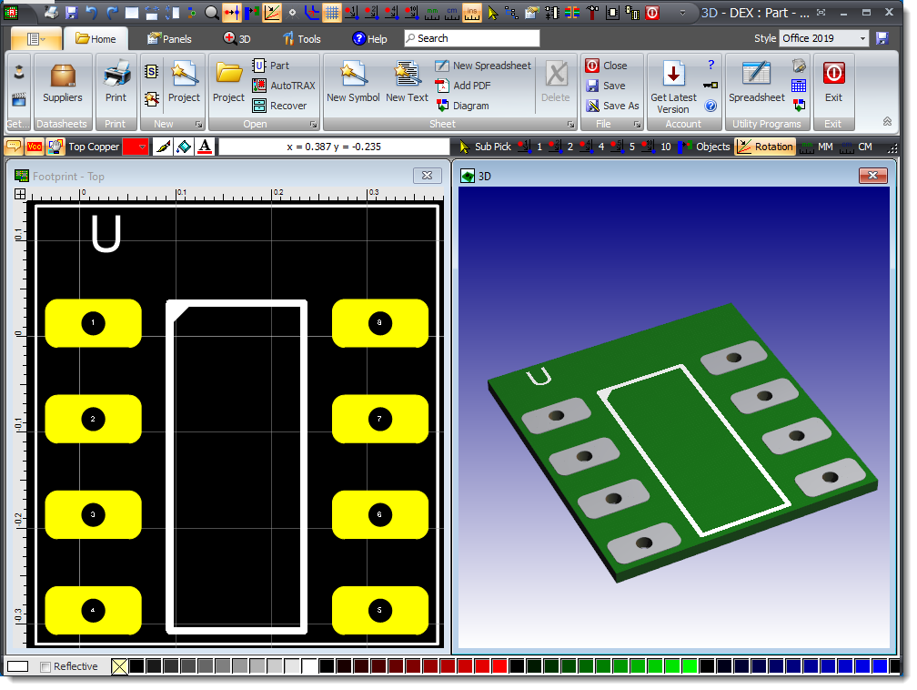
New Colorbar
Monday 6 May 2024
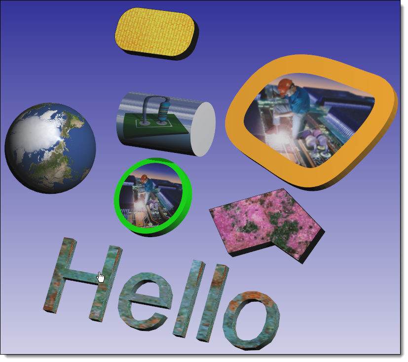
Texture Maps
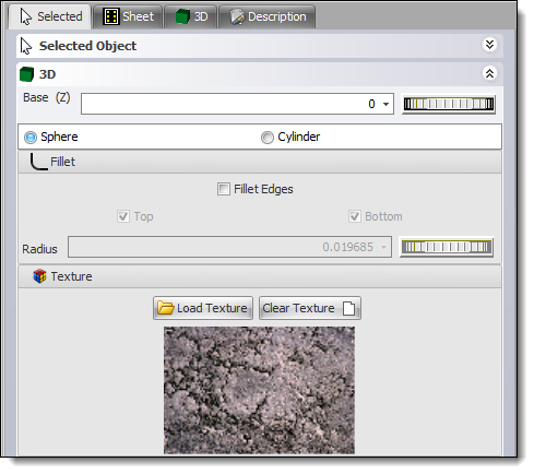
Properties Panel
•Improved automatic 3D pin generation for pads.
•Improved 3D behavior for moved objects in 2D or 3D.
•Fix for transparency image slider updating 3D.
•Improved transparency slider for the image editor.
•Images now remember how much percentage transparency has been applied.
•Fix for setting bitmap transparency
•Improved fillet radius setting for 3D objects
•Pick/View mode saved/restored for 3D viewports.
•Changed shape of 3D ellipses, rectangles now updates the 3D view.
•The following can now have 3D texture-maps when placed on the top or bottom package layers
o lines
o polylines,
o arc,
o rectangles,
o circles and ellipses,
o curves,
o shapes
•Fix for Curve Properties editor not showing assigned layer.
•Fix for DRC strict design rule not restoring if set.
Friday 3 May 2024
Color Bar
Back by popular demand.
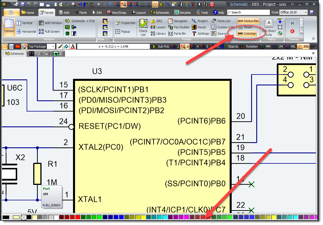
The Color Bar
 Bug Fixes
 •Improved Extrusion Editor
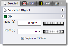
Extrusion Editor
Wednesday 1 May 2024
 Bug Fixes
 •Fix teardrops on tracks.
April
•Tuesday 30 April 2024
 Bug Fixes
 •Fix for the PCB grid transparency not being restored.
•Fix for the differential pair routing if the length of either pair is too short.
•Fix for countries where commas are used for decimal points. For example 1,2 instead of 1.2
•Teardrop buttons behavior fixed.

Teardrops
Sunday 28 April 2024
PCB Holes
for PCB holes in footprints, you can now view/edit the hole's center offset from the footprint's placement point.
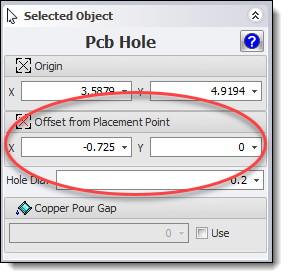
Hole Offset
Pad Names
Now orientation corrected if the footprint/pad is rotated.
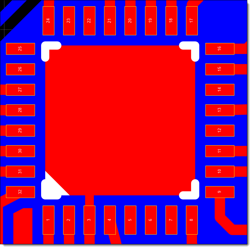
Before
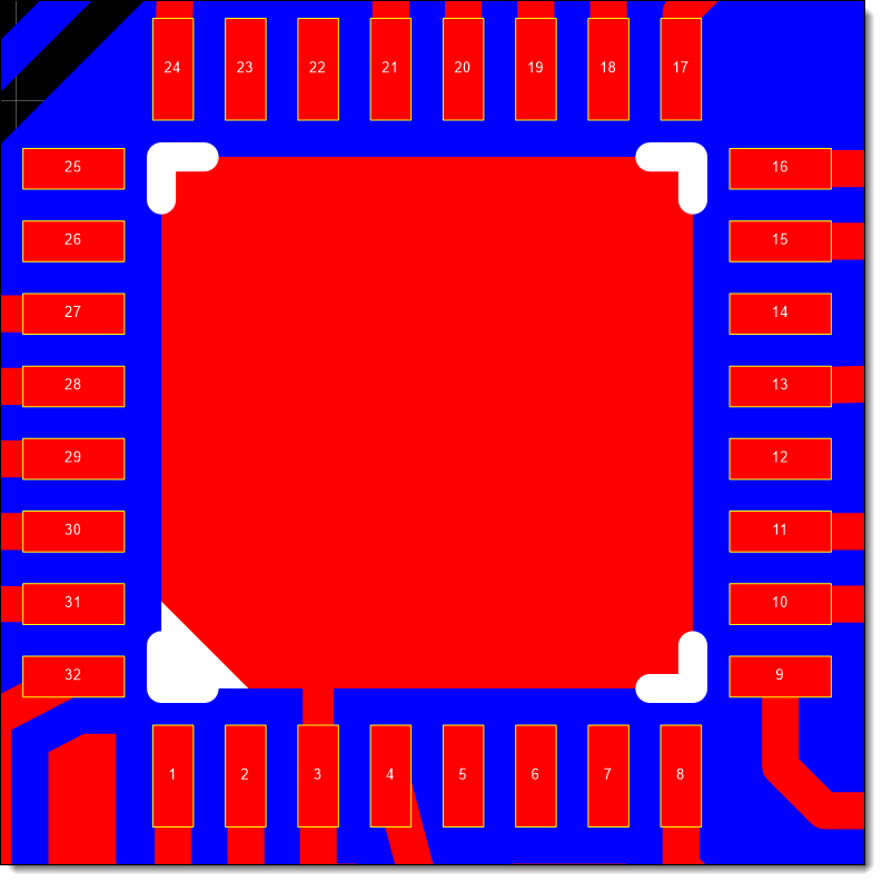
Now: Rotation Corrected
Saturday 27 April 2024
4 Utility Programs
Text Editor
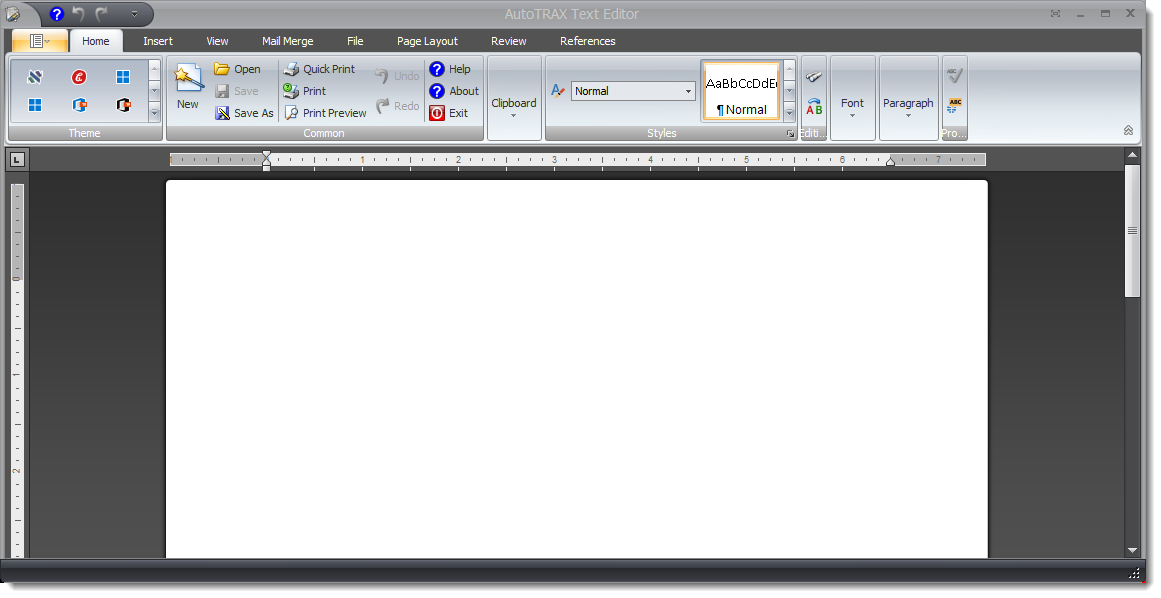
New Microsoft Compatible Text Editor
Spreadsheet Editor
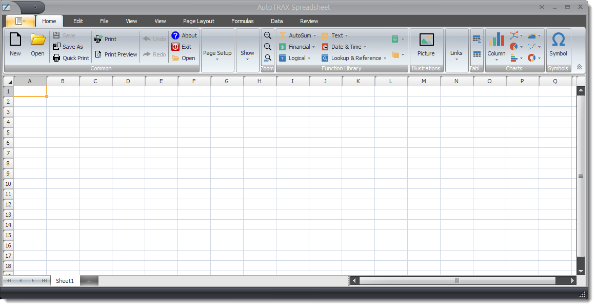
New Microsoft Compatible Spreadsheet Editor
Diagram Designer
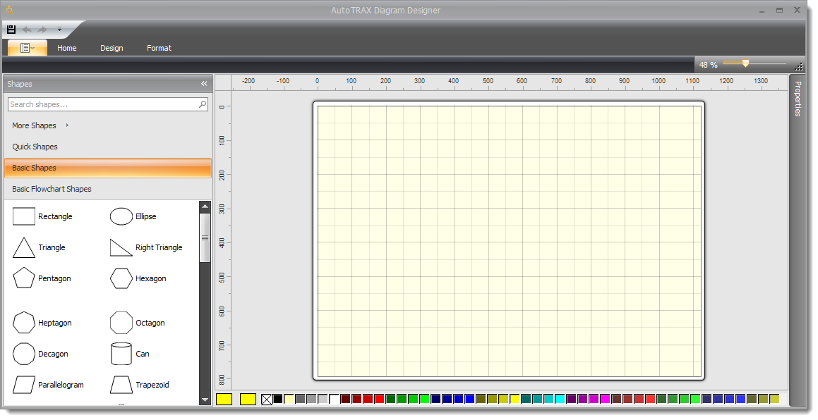
New Diagram Designer
Scheduler
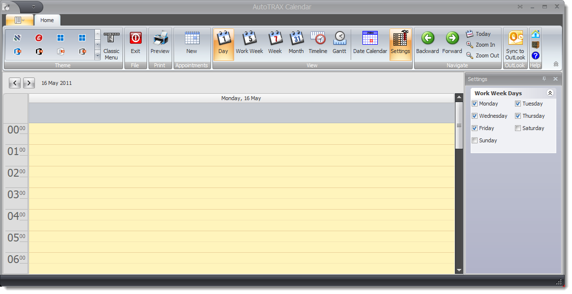
New Scheduler
Friday 19 April 2024
 Fix for the Design Rule Checker
Fixed for checking copper pours with unconnected areas removed.
Thursday 18 April 2024
Multi-Colored Silkscreens
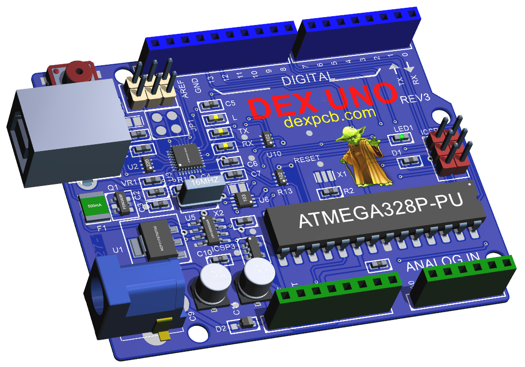
Multi-Colored Silkscreen in 3D
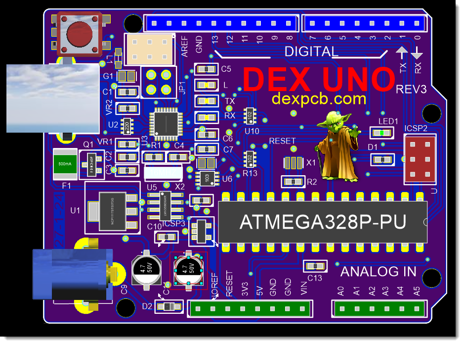
Multi-Colored Silkscreen in 2D
There is now a new option to generate Portable Network Graphic (PNG) files with full RGB+Alpha images at 1200 dpi for both the top and bottom silkscreens. PNG files handle 16 million colors and are both compressed and lossless.
You can add images with transparency!
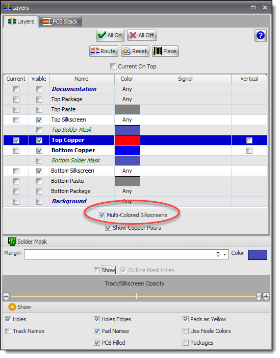
Layers Panel
Sunday 7 April 2024
Setting the Length of a PCB
Setting the Length of a PCB Net
March
Sunday 31 March 2024
Balance Multiple PCB Nets
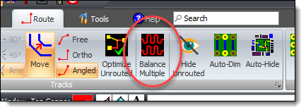
Balance Multiple PCB Nets
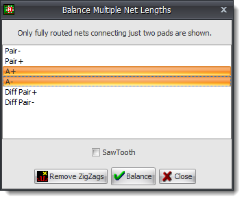
Balance Multiple PCB Nets Dialog
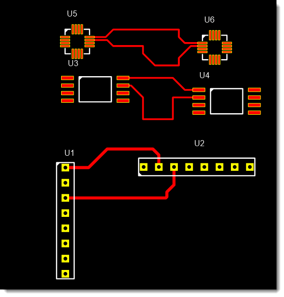
Before Balance Multiple PCB Nets
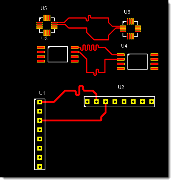
After Balance Multiple PCB Nets
Friday 29 March 2024
 Fix for Default Via Hole and Diameter Settings
Improved Castellated PCB Editor
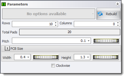
Castellated PCB Editor
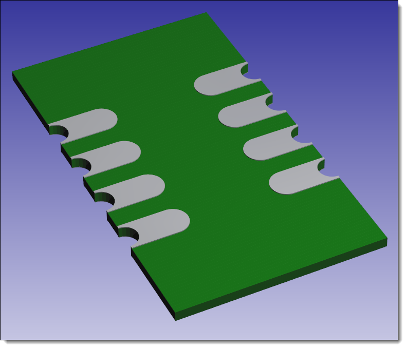
Castellated PCB
Monday 25 March 2024
 Several Minor Internal Bug Fixes
Thursday 14 March 2024
Track Balancing Now Works with Nets with Vias and Short Track Segments
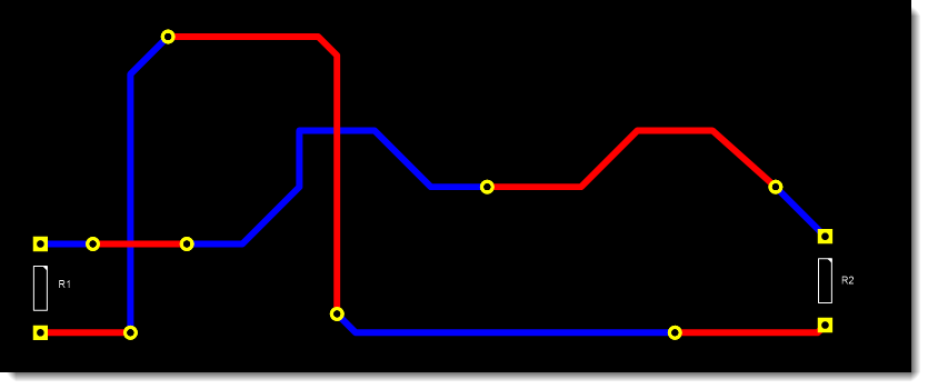
Net Pair with Small Track Segments
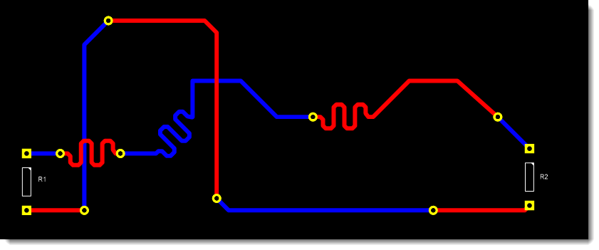
Balanced Net Pair with Small Track Segments
Track Balancing Now Works with Nets with Vias
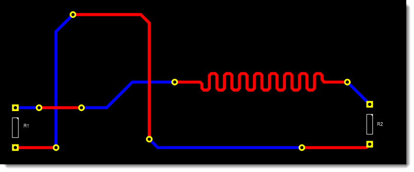
Balanced Net Pair
Wednesday 13 March 2024
 Fix for 3D Base and Depth Thumbwheels Not Updating 3D
3D Base and Depth Thumbwheels
Tuesday 12 March 2024
Added Button to Remove Track Balancing ZigZags

Remove ZigZags
Improved Visibility of Manipulator Points
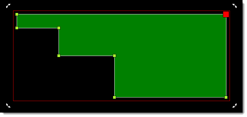
Polygon Manipulator Points
Monday 11 March 2024
Added manually balancing differential track lengths
A differential pair is:
•Two separate PCB nets
•One of the nets must be named <NAME>+
•The other net must be names <NAME>-
▪where <NAME> if the base name e.g. MyNet
▪so example nets are named MyNet+ and MyNet-
•Both nets must only have one track. No junctions or vias.
To Balance
•The two tracks must be fully routed.
•The two tracks must be on the same layer.
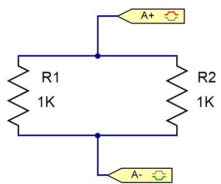
Very Simple Test Differential Pair
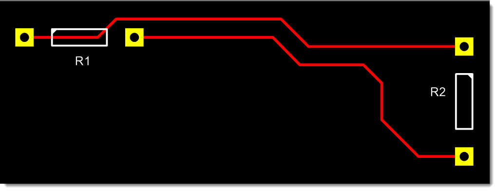
Before Balancing Track Lengths

Balance Command
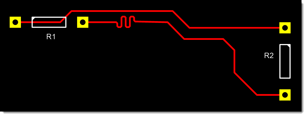
After Balancing Track Lengths
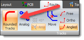
Rounded Track Command
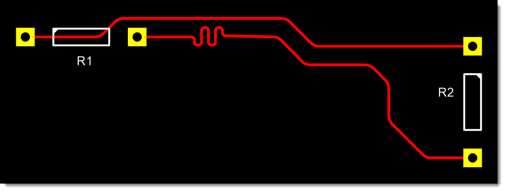
Applying Rounded Tracks
Reassigning Symbol Terminal Pads
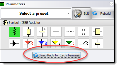
Swap Pads for 2 Terminal Symbols
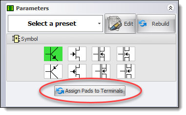
Reassign Pads to Terminal Symbols
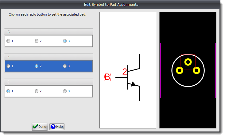
Reassign Pads to Terminal Symbols
Sunday 10 March 2024
Added Send Mail Button

Send Email
Saturday 9 March 2024
Add Block Capacitor to New Part Dialog
Right Click Menu Option in the Library Now Adds New Part
Friday 8 March 2024
New Transistor Symbols
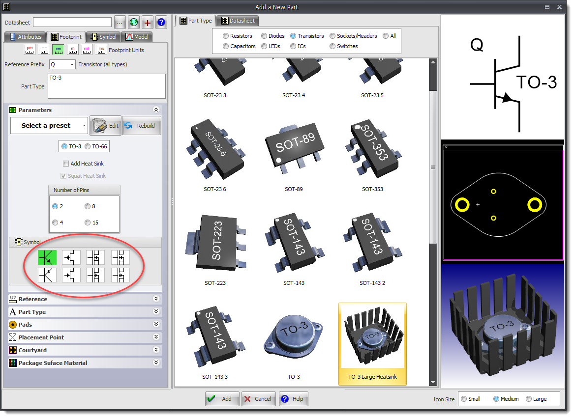
Transistor Symbols
Add Part Dialog and the Spice Model
Now sets the Spice model type.
 Fix for Parametric Editor Not Updating All Controls
Monday 4 March 2024
 Fix for E6 Resistor Color Bands
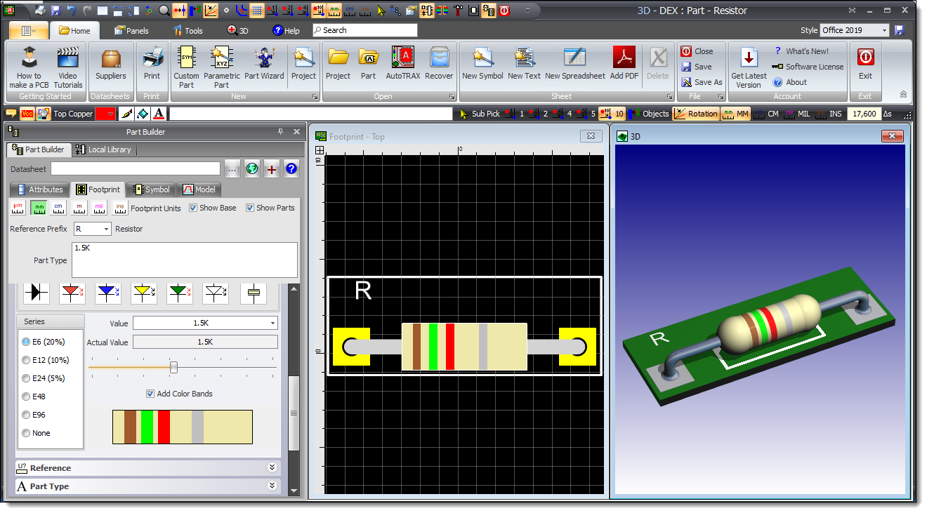
Resistor Color Bands (E6)
2D Viewports - Center View at Mouse Cursor Position - F5
Pressing F5 will center the view at the mouse cursor position, and will move the mouse cursor to the center of the viewport.
IEEE and IEC Resistor Symbols
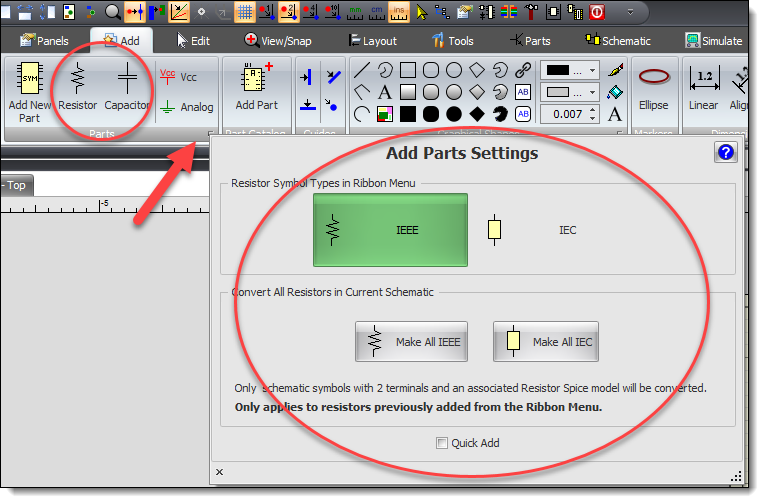
Changed Menu
Part Wizard Removed
Function better implemented in the New Part Dialog. This makes the user interface more consistent.
New Add Resistor Dialog
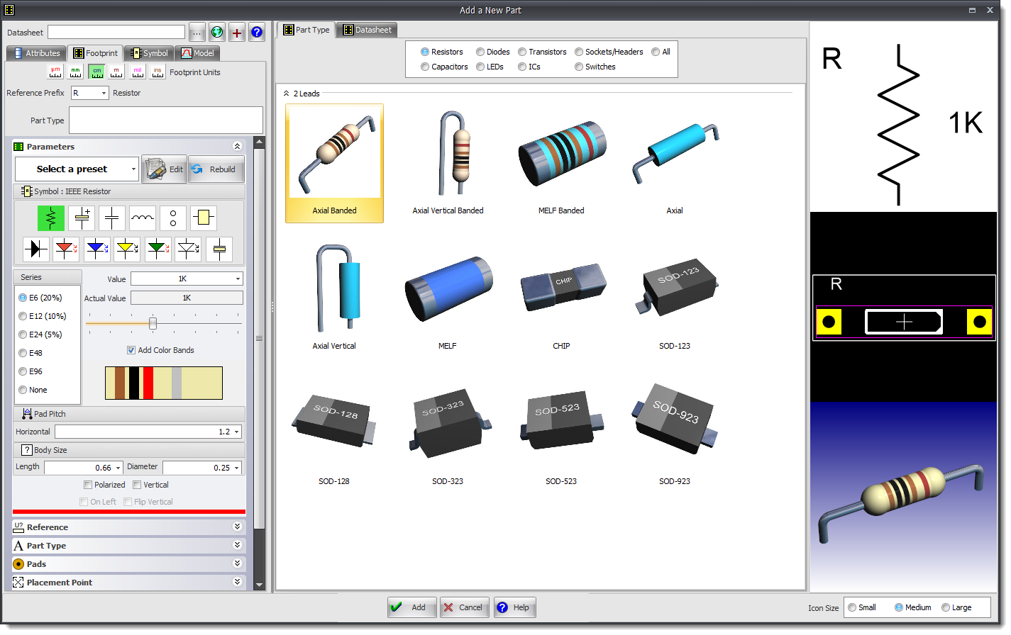
Add Resistor Dialog
New Add Capacitor Dialog
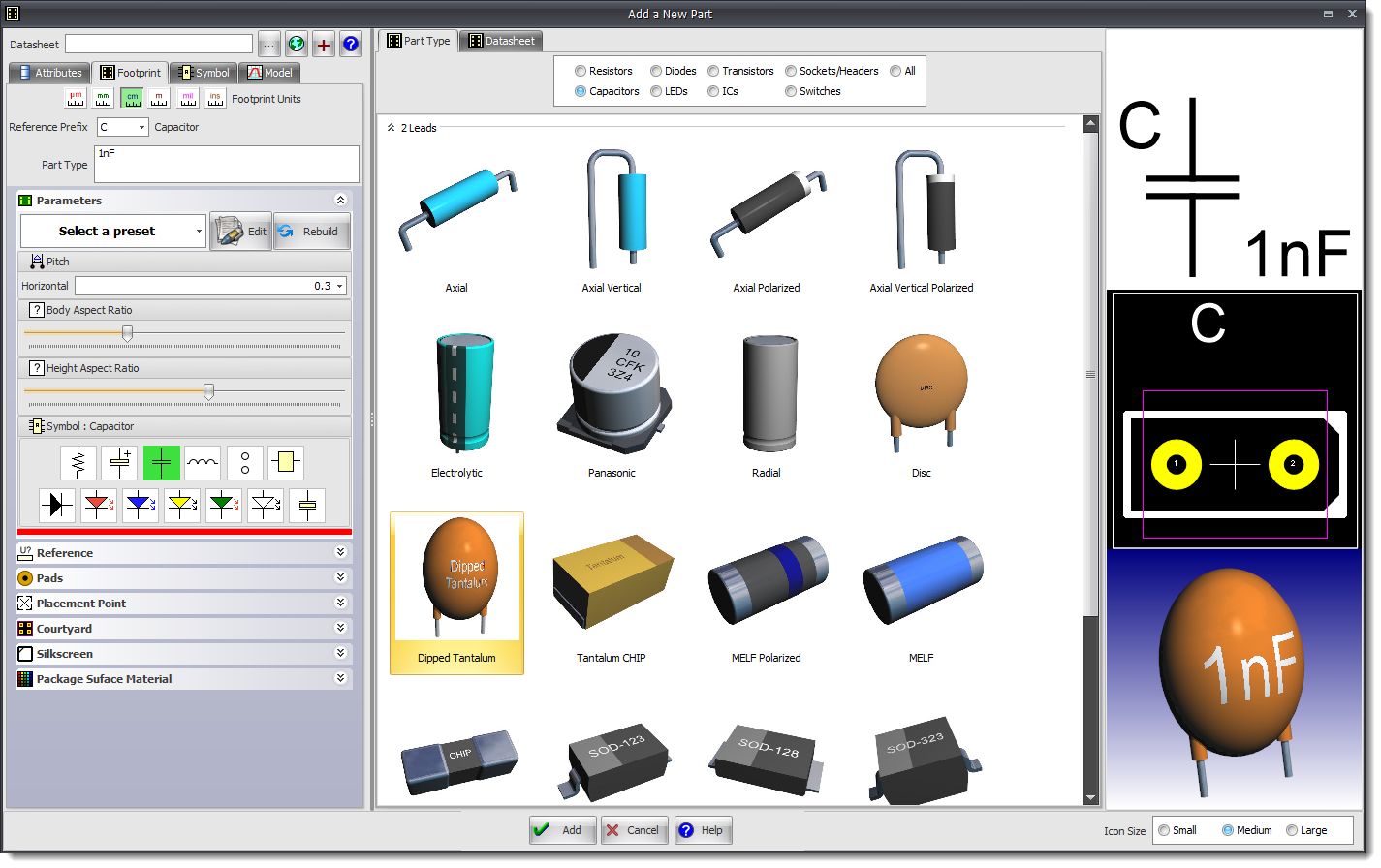
Add Capacitor Dialog
Plotting - Saving Toner
By default, when plotting negative, black toner does not fill the page: saving you on toner costs. Check the restrict column.
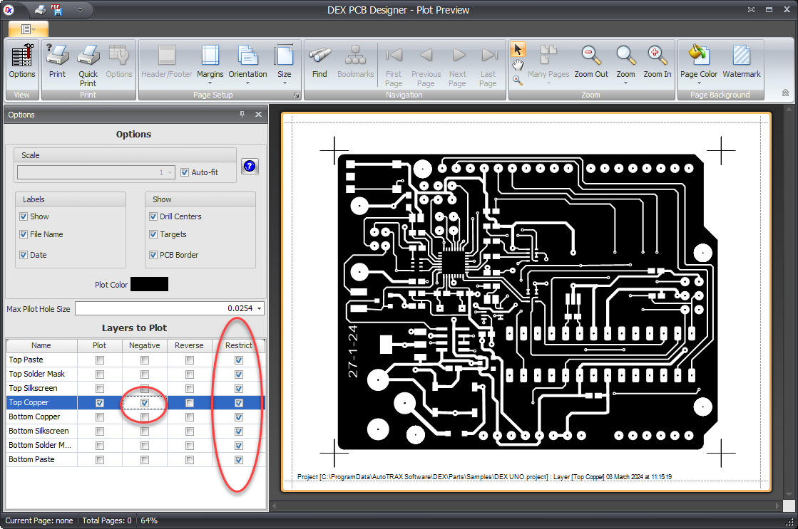
Plotting
Friday 1 March 2024
Grid Strength
You can now set the strength of the grid in viewports. These sliders change the transparency of the grid.
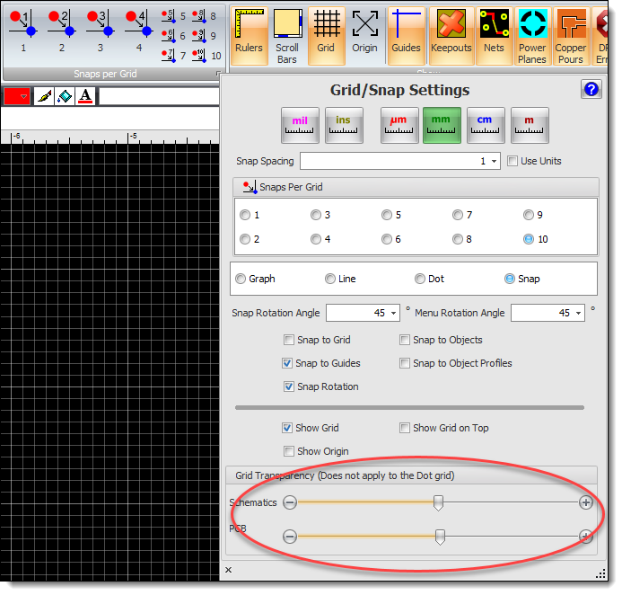
Grid Settings
 Add Resistor and Add Capacitor Dialog
The 3D viewports did not show on the second showing of the dialog.
New layout for the Add Capacitor dialog.
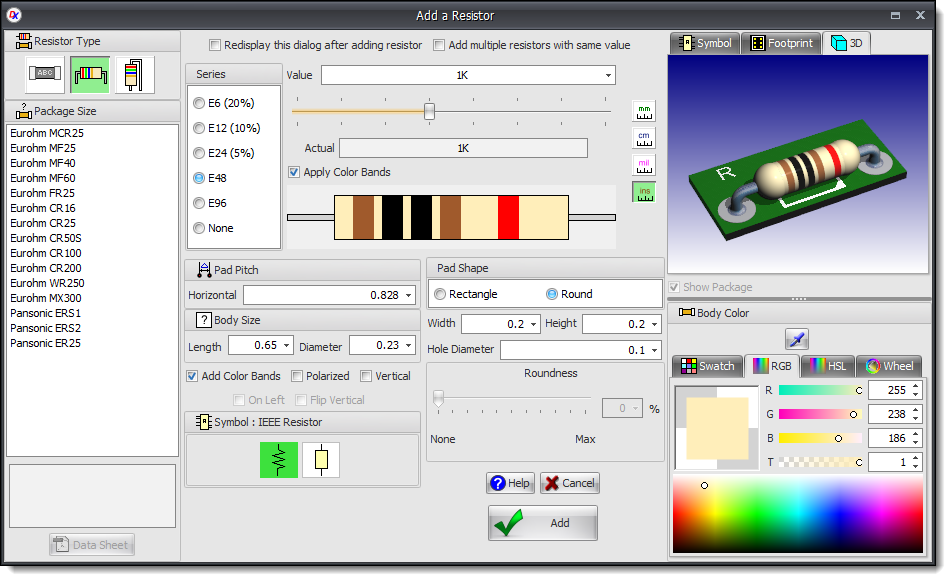
Add Resistor Dialog
New layout for the Add Capacitor Dialog
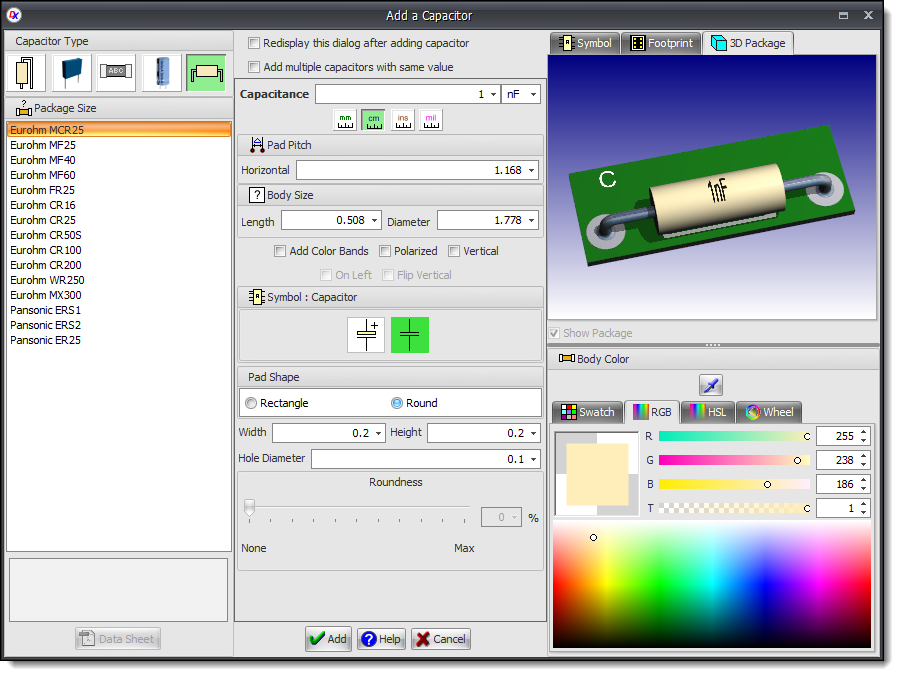
Add Capacitor Dialog
February
Thursday 29 February 2024
Collada 3D Import
Improved import. Models combined into 1one selectable object.
Pad Properties Editor
Added thumbwheel controls for pads size and hole size.
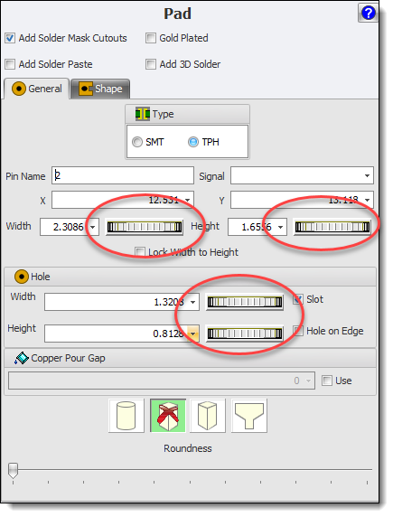
Pad Properties Editor
Add Capacitor Dialog
Redesigned to be more consistent with the Add Resistor Dialog.
 Fix for adding schematic wires to existing schematic node.
Added track was not set to the correct width.
 Track Properties Editor
Thumbwheels (track widths) were initially not working as expected.
 Footprint Silkscreens
Some older parts had rectangular silkscreens added when no silkscreen should have been added.
Wednesday 28 February 2024
 Fix for terminals list for parts without terminal magnets not displaying.
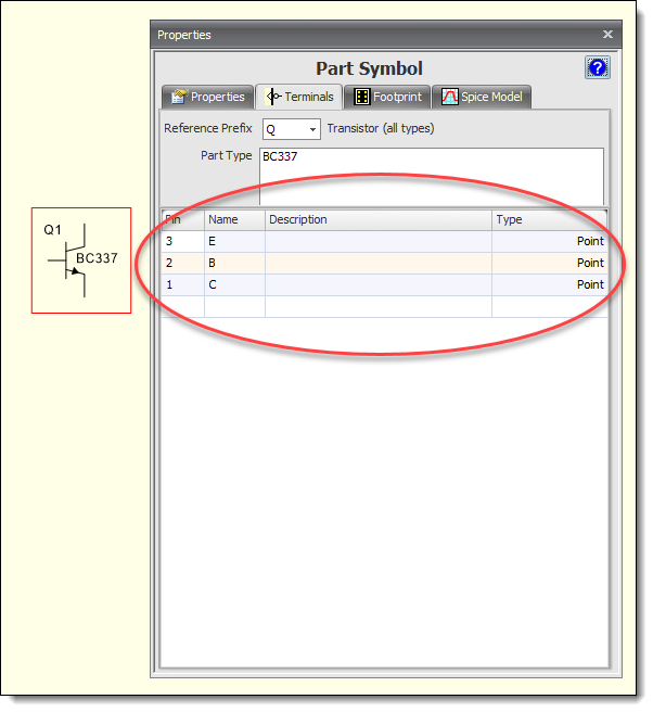
Footprint Properties Popup (F2)
Tuesday 27 February 2024
 Fix for some Eagle libraries not importing.
Monday 26 February 2024
 Fix for apparent dangling tracks when the 'End' pressed when manually routing.
Track not really 'dangling' : just an error in not drawing unrouted segment.
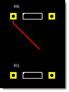
Dangling Track
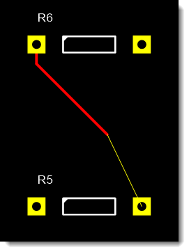
Fixed
You can also press the End key.
 Fix for manually routing from SMT pads would sometimes undo the route on left click.
This would make routing sometimes very difficult.
 Fix for double click to end adding copper pours.
You can also press the End key.
Sunday 25 February 2024
 Fix for Floating Viewports Not Receiving Ribbon Menu Commands
The floating viewport show the"Active Viewport" message in it's caption if it has focus.
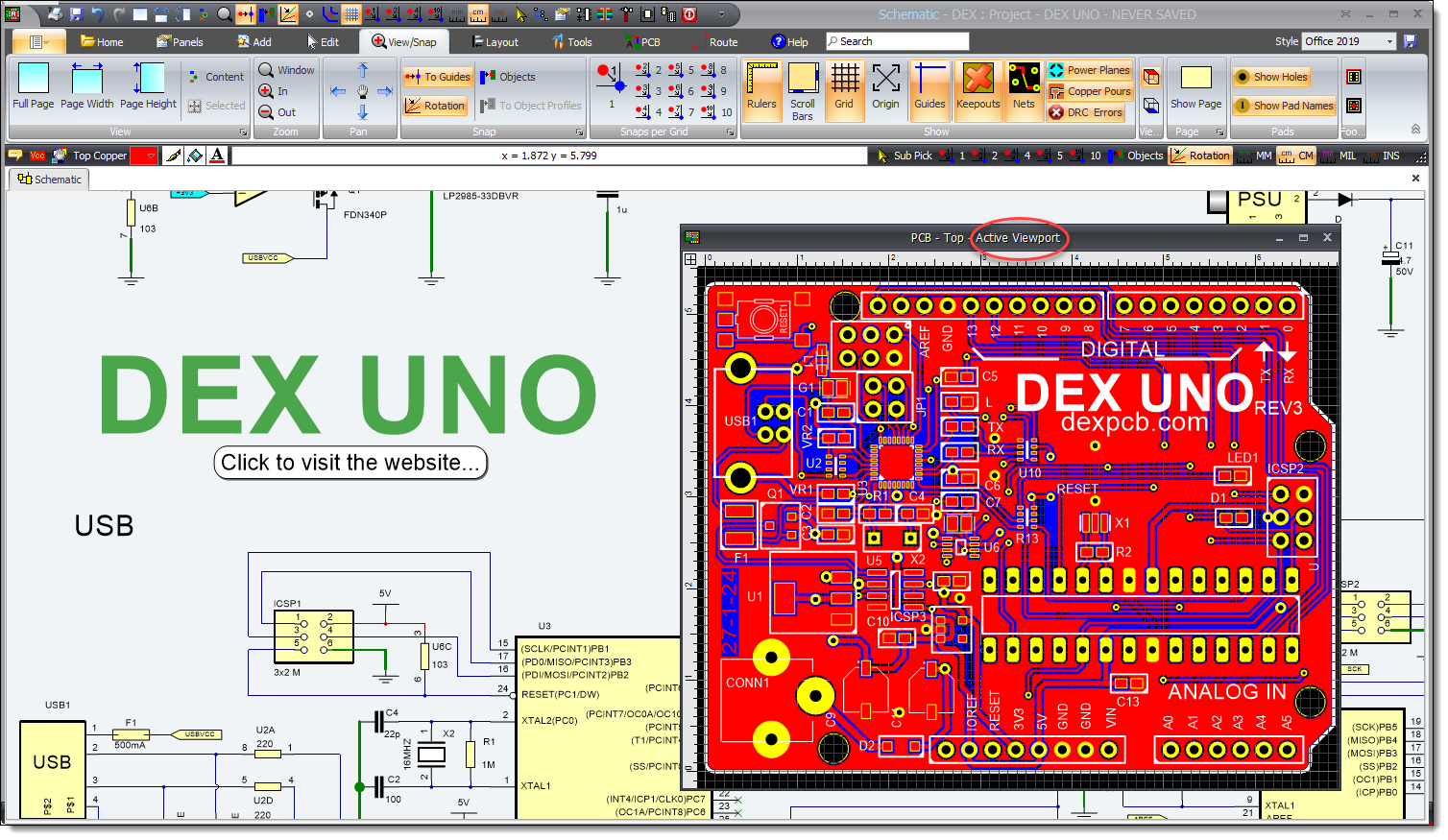
Floating PCB Viewport
Optimized Footprint Properties Dialog
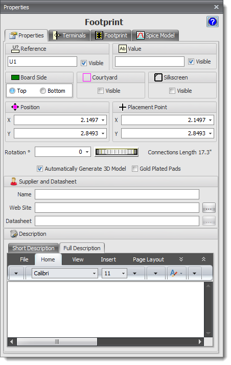
Footprint Properties Dialog
Saturday 24 February 2024
Rounded Corners for 3D Tracks
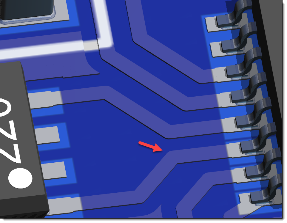
Rounded Corners for 3D Tracks
Thumbwheel Controls to Set Track Widths
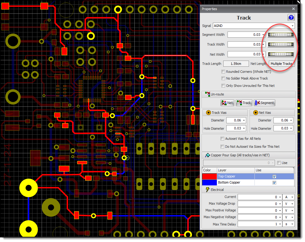
Thumbwheel Controls to Set Track Widths
Friday 23 February 2024
 Fix for Symbol Buttons in the Add Resistor Dialog and Add Capacitor Dialog
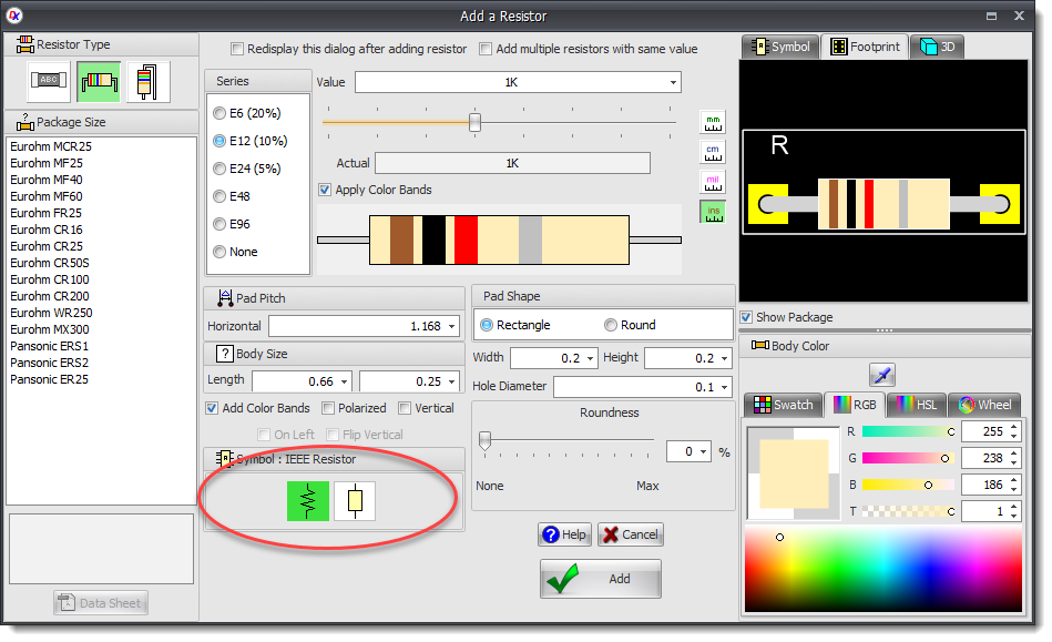
Add Resistor
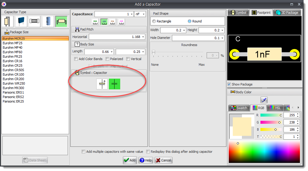
Add Capacitor
•Fixed some bugs where via sizes incorrectly sized when manually routing.
•Improved Track Properties Editor.
•Improved Via Default Properties Editor.
Pad Properties Editor
Optimized and eliminated/simplified controls not relevant for the pad settings e.g. SMT and TPH.
Similar optimizations have been down on all the other entity properties editors (a total of 85 editors).
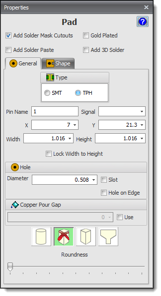
Pad Properties Editor
Thursday 22 February 2024
Images
All images converted to 32 bits when pasting or importing from files.
Images now pickable in the Part Editor - no need to sub-pick.
Image Editor
Transparency changes in real-time when dragging the transparency slider.
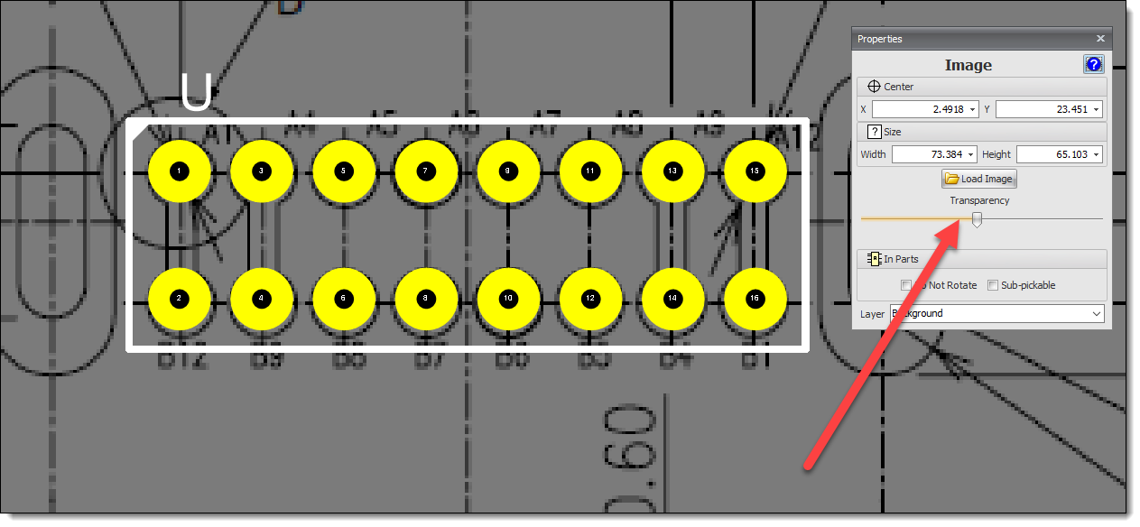
Background Image with Transparency
Image copied from a datasheet using Screen Capture and pasted onto the Background layer. Great for using as a tracing background when adding pads in fully custom parts.
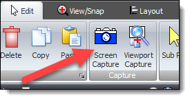
Screen Capture
 Fix for numeric entry fields losing focus when entering text.
 Fix for via sizes when manually re-routing.
Wedneday 21 February 2024
Fix for Fill Editor not Updating Correctly
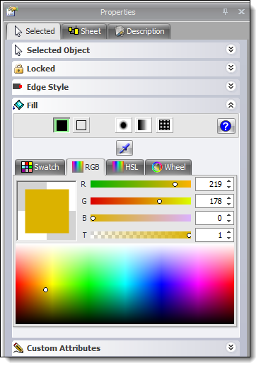
Fill Editor
Fix for the Font Editor Thumbwheel not Refreshing the Viewport
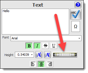
Font Height Thumbwheel
Tuesday 20 February 2024
Improved UI Control Layout
Several dialog layouts improved. e.g. the Track Properties Editor.
 Fix for Track Via Diameters and Hole Sizes
•Fixed some bugs where via sizes incorrectly sized when manually routing.
•Improved Track Properties Editor.
•Improved Via Default Properties Editor.
Monday 19 February 2024
Added Full Screen Menu Button
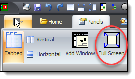
Full Screen Menu Button
Sunday 18 February 2024
Two Main Windows for Dual Monitors
You can view the schematic on the left monitor and the PCB on the right. Try out the Navigator and cross selection.
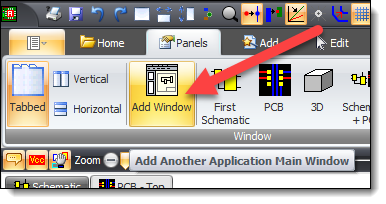
Adding Another Window

Two Main Windows Viewing the Same Project
The schematic on the left monitor and the PCB on the right monitor.
Properties Popup Panel
The popup properties panel has been improved and works in full-screen mode (F11)
Full-Screen
Press Ctrl + F11 to display full screen over all your monitor screens.

Full-screen with 2 horizontally aligned monitors.
Thursday 15 February 2024
 Switching Between Tiled and Tabbed Viewports
AutoTRAX DEX sometimes crashed! This should now be fixed.
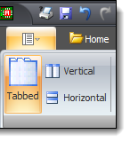
Viewports
Wednesday 14 February 2024
Properties Popup Panel
The popup properties panel has been improved with removal of non-applicable controls and better resizing of the pen and fill editors.
Thursday 8 February 2024
Properties Popup Panel
Press F2 to show/hide the Properties Popup Panel
Wednesday 7 February 2024
Properties Panel
Improved pen editor. Redundant controls not displayed.
Improved fill editor. Redundant controls not displayed.
Properties Popup Panel

Popup Properties
Improved layout.
Reorganized Panels button group.
Hide on item move.
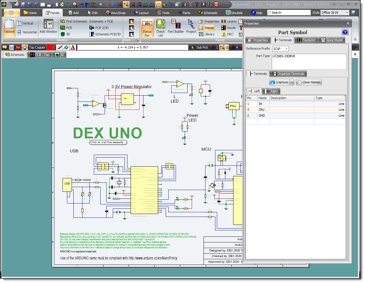
Popop Properties Panel
Friday 2 February 2024
 Organize Symbol Terminals
Fix for organizing symbol terminals. (some minor errors).
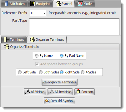
Organize Terminals
Thursday 1 February 2024
Create a New Part Dialog
Added Mouser button to search and add datasheet.
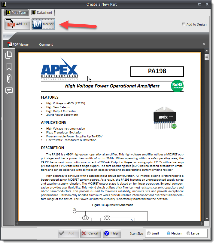
Create a New Part
January
Sunday 28 January 2024
Wire Junction Points (Optional)
Wire Junction Points now added to the end of symbol terminals with more than one connection.
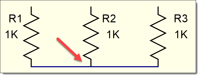
No Wire Junction Point
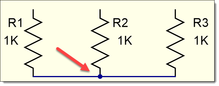
With Wire Junction Point
Saturday 27 January 2024
Status Bar
Improved behavior of the Status Bar.

Status Bar
Thursday 25 January 2024
Layers Panel
Improved behavior for Route/Reset/Place buttons.
Added Show Copper Pour checkbox.
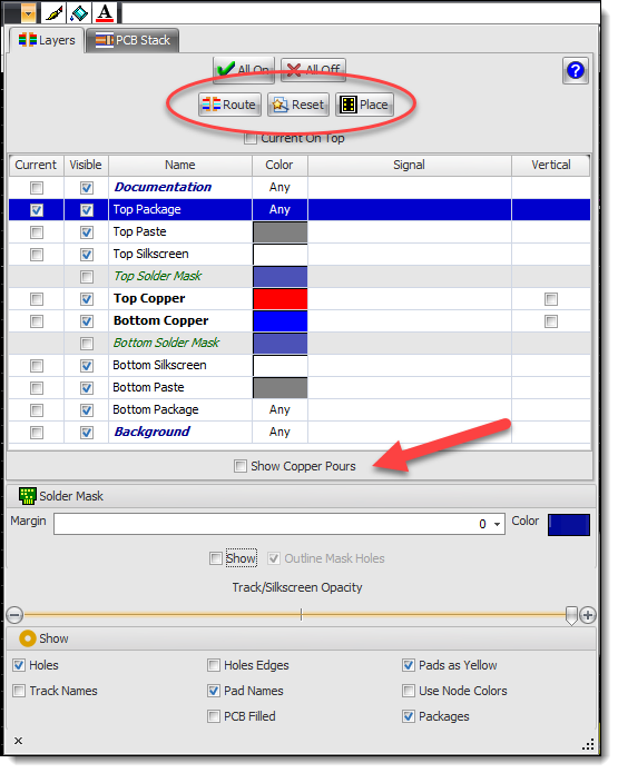
Layers Panel
Grid/Snap Settings Popdown Editor
Added extra commands.
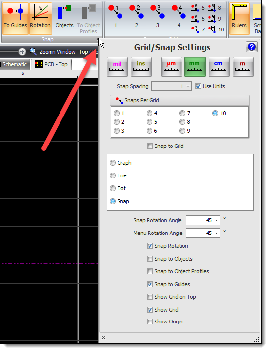
Grid/Snap Settiings Popdown Editor
Undo/Redo Design State Manager
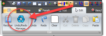
Undo/Redo
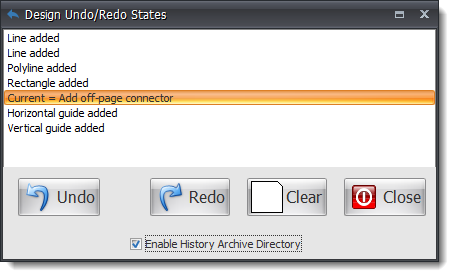
Undo/Redo Design State Manager
Tuesday 23 January 2024
 Printing
Fix for 3D view from bottom and view from top not working.
Monday 22 January 2024
 Setting Image Transparency
Fix for setting the transparency of images pasted from the clipboard using the properties panel.
 Add Resistor Dialog
Fix for disabled pad shape editor.
Markers
Improved graphics.
Draws in multiple colors, even on PCB copper layers. NOTE: do not add them to copper layers, use the Documentation layer (top most)
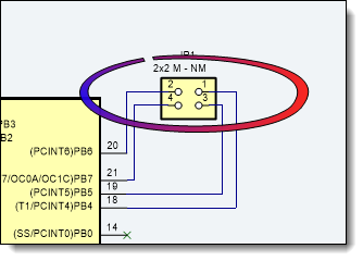
A Marker
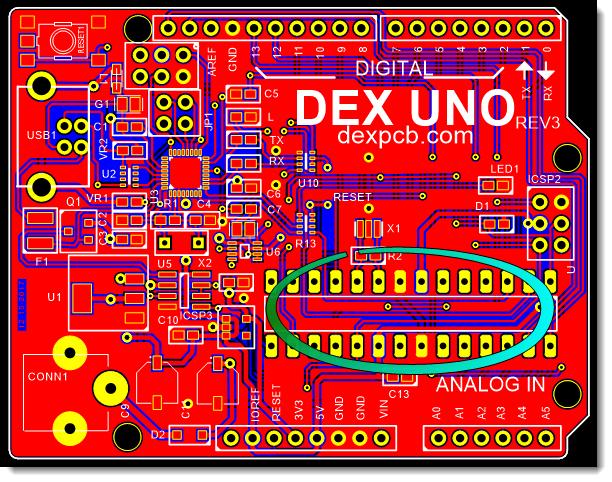
A Marker in a PCB
Sunday 21 January 2024
Part Renumbering
Redesign of the part renumbering panel.
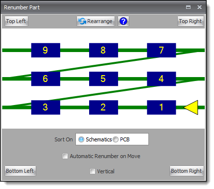
Part Renumbering Panel
Saturday 20 January 2024
CNC Output
Text now supported. (stick text).
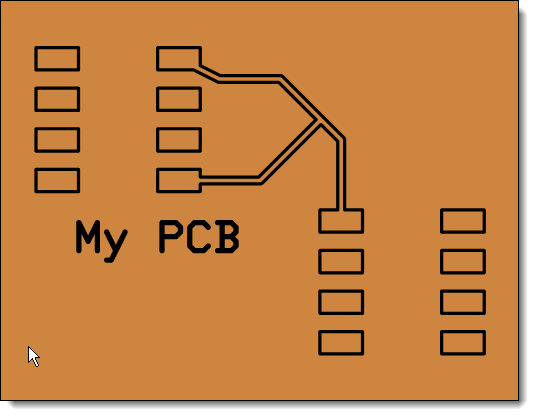
CNC Text
Horizontal and Vertical Tiled Viewports
Automatic resizing to eliminate blank areas.
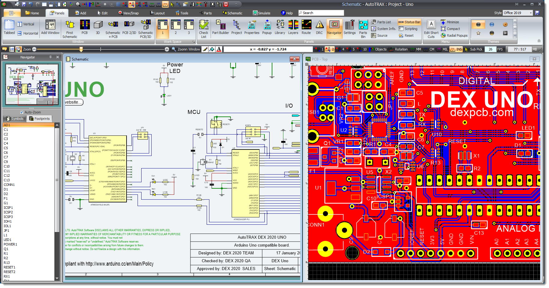
Vertical Tiled Viewports
Sunday 14 January 2024
SMD Automatic Connections
Split Power Planes
Automatic connection to power planes for SMD pads. (Route Menu)
Power Planes
Automatic connection to power planes for SMD pads and TPH pads. (Route Menu)
Design Rule Checker and Split Power Planes
Checks for connections to split power planes.
Thursday 11 January 2024
Split Power Planes
Improved automatic via connections from SMT pads to internal split power planes.
Power Planes
Improved automatic via connections from SMT pads to internal power planes.
Wednesday 10 January 2024
Layers Panel
View/Hide Unrouted Tracks.
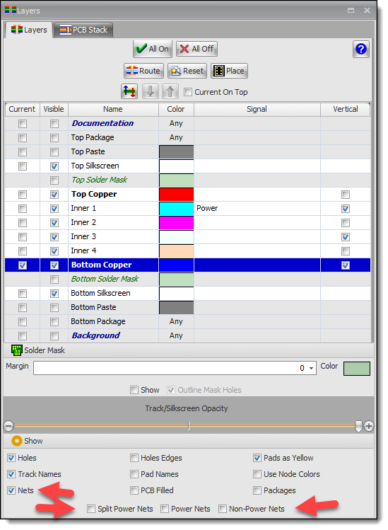
View/Hide Unrouted Tracks
Tuesday 9 January 2024
Color Bar Panel
The Color-Bar panel at the bottom of the viewport has been removed. It takes up too much screen space. Use the line, fill, and text properties buttons  in the Status bar.
You can also use the selected properties panel.
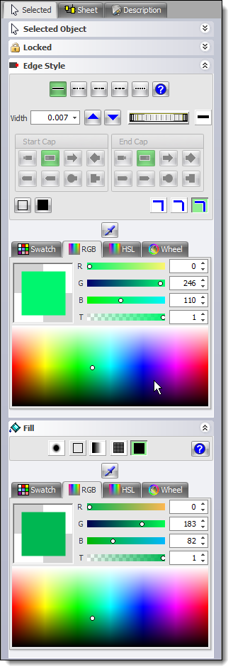
Setting Line and Fill Properties
Layers Panel
Improved layout and functionality.
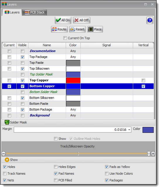
Layers Panel
Track Properties Editor
Improved layout and functionality.
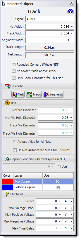
Track Properties Editor
Sheet Properties Editor
Improved layout and functionality for the PCB.

Sheet Properties Editor
Thursday 4 January 2024
DRC Checker
Now works with PCB tracks with narrow/wide sections.
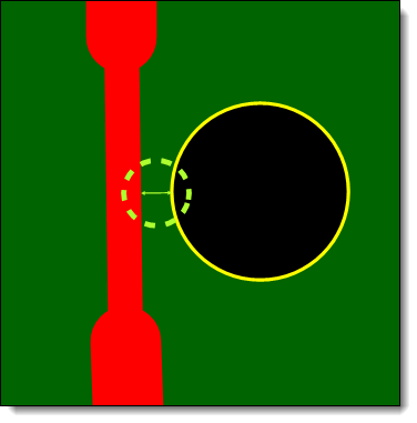
Track to PCB Hole Error
Wednesday 3 January 2024
New Track Edit Dialog.
Improved layout and behavior.
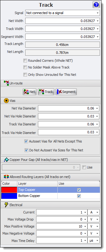
Track Properties Editor
Tuesday 2 January 2024
Clear All Ignore Autoset Vias on All PCB Nets.
Only enabled if any PCB nets are set to ignore autoset vias.
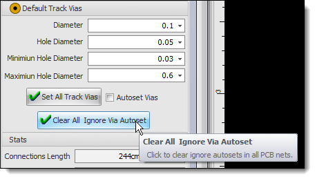
Monday 1 January 2024
Track Widths
Simplified track width setter:

Set All Track Widths / Default Track Width
Auto-sizing of Track Vias
Simplified via size setting.
Use Autoset Vias to automatically set all via diameters, and via hole diameters based on connected tracks.
This can be overridden for individual PCB net: see below.
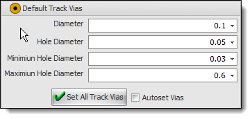
Setting Via Sizes
Auto-PCB Net - Ignore Automatic Via Sizing
Check to ignore automatic via sizing for individual PCB nets.
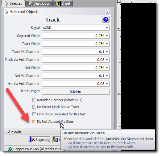
Ignore Autoset via sizes for individual nets.