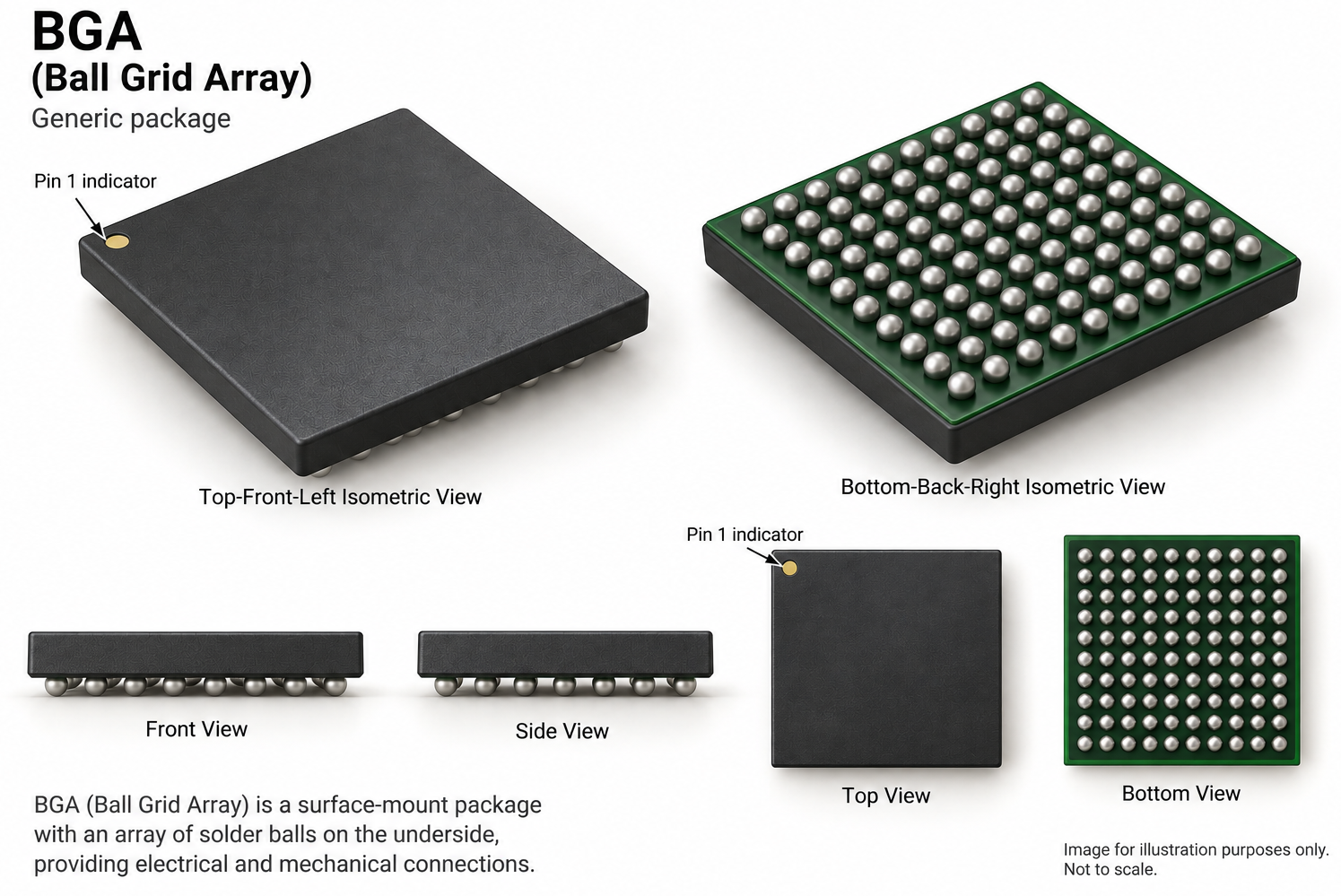
A Generic BGA
What is a BGA (Ball Grid Array)?
A BGA (Ball Grid Array) is a surface-mount integrated circuit (IC) package that uses a grid of small solder balls arranged underneath the package body to provide electrical and mechanical connections to a printed circuit board (PCB).
Unlike traditional IC packages such as DIP, SOIC or QFP, which have leads extending from the sides of the package, a BGA places its electrical connections directly beneath the component. This arrangement allows a significantly greater number of connections within a relatively compact area, making BGA packages particularly suitable for complex, high-performance integrated circuits.
Construction and characteristics
A typical BGA consists of a moulded plastic or ceramic body containing one or more semiconductor dies, an internal interconnection structure, and an array of solder balls attached to its underside.
The solder balls are arranged in rows and columns, usually at a uniform pitch. During PCB assembly, the component is positioned over matching copper pads and heated in a reflow oven. The solder balls melt and form permanent electrical and mechanical connections between the IC and the PCB.
Common characteristics include:
•Mounting type: Surface-mount technology (SMT).
•Terminal configuration: Two-dimensional array of solder balls beneath the package.
•Ball counts: From a few dozen to several thousand, depending on the device.
•Typical ball pitches: 0.35, 0.40, 0.50, 0.65, 0.80, 1.00 and 1.27 mm, although other pitches are available.
•Body materials: Plastic, organic laminate or ceramic, depending on the package construction.
•Ball arrangement: Full rectangular grid, perimeter-only array or partially populated grid.
•Pin identification: Ball positions are commonly identified using alphanumeric coordinates, such as A1, B1 and C1, rather than consecutive pin numbers.
Advantages
BGA packages provide several important advantages over conventional leaded IC packages.
Their underside connection arrangement supports high terminal densities without requiring extremely fine-pitch leads around the package perimeter. The relatively short electrical connections can reduce parasitic inductance and improve signal integrity, making BGAs particularly suitable for high-speed digital circuits.
The large number of available connections also allows designers to allocate additional terminals to power and ground, improving power distribution and potentially reducing electrical noise.
Depending on the package construction, BGAs can also provide effective thermal conduction through their solder connections and internal substrate.
Disadvantages
The principal disadvantage of BGA technology is that its solder joints are concealed beneath the package after assembly. Consequently, conventional visual inspection cannot reliably determine whether every connection has been formed correctly.
Specialised inspection methods, such as X-ray inspection, are frequently used to identify solder bridges, missing balls, voids and other assembly defects.
BGA components also require accurate PCB footprints, controlled solder-paste application, suitable reflow profiles and careful PCB layout. Replacing or repairing a BGA generally requires specialised rework equipment.
Applications
BGA packages are widely used in modern electronic equipment, including microprocessors, graphics processors, memory devices, FPGAs, high-performance microcontrollers, communications processors and system-on-chip devices.
They are particularly valuable where high connection density, compact dimensions and good electrical performance are required.
PCB design considerations
When creating a BGA footprint in AutoTRAX DEX, the designer must account for the package body dimensions, ball diameter, horizontal and vertical ball pitch, row and column arrangement, missing-ball positions, and the manufacturer's recommended PCB land pattern.
Unlike packages with conventional numbered leads, BGA terminals commonly use alphanumeric identifiers. For example, terminal A1 identifies a particular ball position, while B1 identifies another position in the grid.
The package's physical ball arrangement must correspond exactly with its electrical pinout. Even a single incorrectly positioned or identified ball can result in an unusable PCB or damage to the device.
Important: BGA footprints should always be generated or verified using the manufacturer's official package drawing and recommended land-pattern specifications. Generic BGA dimensions must not be assumed to apply to a particular IC.