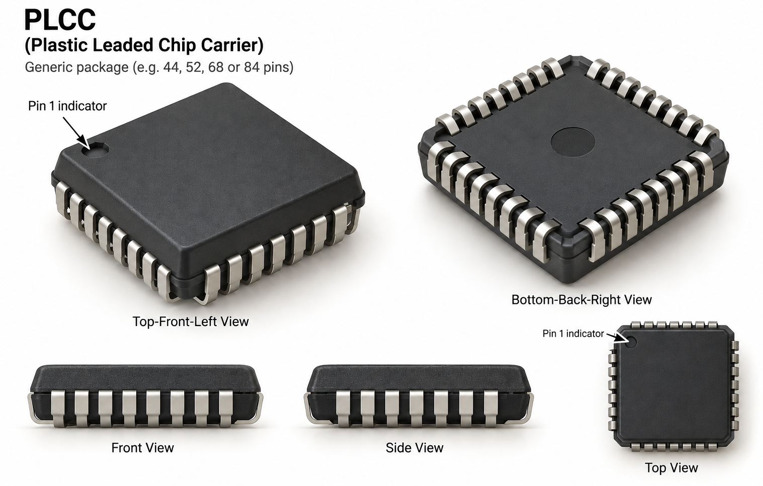
A Typical PLCC IC
What is a PLCC?
A PLCC (Plastic Leaded Chip Carrier) is a surface-mount integrated circuit (IC) package featuring a square or rectangular moulded plastic body with metallic J-shaped leads arranged around all four sides.
Unlike conventional DIP packages, which have straight pins extending downwards, PLCC packages use leads that curve underneath the package body. This distinctive arrangement produces a compact, mechanically robust package suitable for direct PCB mounting or insertion into a compatible PLCC socket.
Main characteristics
•Construction: Moulded plastic body protecting the semiconductor die.
•Lead configuration: J-shaped metallic leads extending from all four sides and curling underneath the body.
•Pin counts: Common configurations include 20, 28, 32, 44, 52, 68 and 84 pins.
•Lead pitch: Typically 1.27 mm (0.050 inches).
•Mounting: Surface-mount soldering or installation in a dedicated PLCC socket.
•Pin identification: A chamfered corner, moulded dot or other marking identifies pin 1.
•Applications: Microprocessors, microcontrollers, memory devices, programmable logic devices and interface controllers.
Advantages
PLCC packages provide a relatively high number of electrical connections within a compact footprint. Their J-shaped leads offer mechanical compliance that helps accommodate differences in thermal expansion between the IC package and PCB.
Unlike many other surface-mount packages, PLCC devices can also be installed in sockets, allowing convenient replacement, testing and firmware upgrades without desoldering.
Disadvantages
The J-shaped leads are partially concealed beneath the package, making solder-joint inspection and rework more difficult than with packages featuring outward-projecting leads.
PLCC packages are also generally larger and less space-efficient than modern fine-pitch QFP, QFN and BGA packages.
PCB footprint considerations
When designing a PLCC footprint in AutoTRAX DEX, the number of pins, lead pitch, body dimensions, lead geometry and recommended solder-pad dimensions must be obtained from the manufacturer's mechanical specifications.
Important: Although 1.27 mm is the standard lead pitch for many PLCC packages, pad dimensions and package geometry must be verified for the specific device.
PLCC packages remain particularly relevant for legacy microprocessors such as the Zilog Z180, memory devices and programmable logic ICs.
PLCC (Plastic Leaded Chip Carrier) is also known by several alternative names and related package designations used by semiconductor manufacturers.
Name / Abbreviation |
Full name |
Description |
|---|---|---|
PLCC |
Plastic Leaded Chip Carrier |
Standard designation for a plastic IC package with J-shaped leads on all four sides. |
P-LCC |
Plastic Leaded Chip Carrier |
Alternative spelling of PLCC. |
PLCC-J |
Plastic Leaded Chip Carrier, J-Lead |
Descriptive designation emphasising the J-shaped leads. |
JLCC |
J-Leaded Chip Carrier |
General designation for chip carriers with J-shaped leads; may include non-plastic packages. |
PCC |
Plastic Chip Carrier |
Generic designation sometimes used for plastic chip carriers; lead configuration must be checked. |
PQCC |
Plastic Quad Chip Carrier |
Alternative designation sometimes used for four-sided plastic chip carriers. |
QFJ |
Quad Flat J-Leaded Package |
JEITA-style package classification for four-sided J-leaded ICs. |
QFJ-G |
Quad Flat J-Leaded, Gull-Wing Variant |
Not a standard synonym for PLCC; gull-wing leads are a different geometry. |
LCC |
Leaded or Leadless Chip Carrier |
Ambiguous abbreviation. Often refers to a leadless chip carrier, so it should not automatically be treated as PLCC. |
CLCC |
Ceramic Leadless Chip Carrier |
Related ceramic package, normally without projecting leads; not equivalent to PLCC. |
Important: Package aliases are not necessarily interchangeable. Always verify the lead geometry, pin count, pitch, body dimensions, and manufacturer-specific mechanical drawing before treating two package designations as equivalent.