A via is a hole that is used to form an electrical connection between two signal layers of a PCB. Vias are like round pads, which are drilled and usually through-plated when the board is fabricated.

A through-hole via
A typical Via
There are 2 types of vias in AutoTRAX DEX.
Automatic Vias
The first type of via is one that is automatically created by a track in order to switch layers.
Manually Created Vias
The second type of via is one created by you to provide an electrical connection between layers.
A via consists of two pads, in corresponding positions on different layers of the board, that are electrically connected by a hole through the board. The hole is made conductive by electroplating, or is lined with a tube or a rivet. High-density multi-layer PCBs may have micro vias: blind vias are exposed only on one side of the board, while buried vias connect internal layers without being exposed on either surface. Thermal vias carry heat away from power devices and are typically used in arrays of about a dozen.
A via consists of:
•Barrel — a conductive tube filling the drilled hole
•Pad — connects each end of the barrel to the component, plane or trace
•Antipad — a clearance hole between barrel and no-connect metal layer
A via may be at the edge of the board so that it is cut in half when the board is separated; this is known as a castellated hole and is used for a variety of reasons, including allowing one PCB to be soldered to another in a stack.
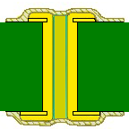
 Through hole. (2) Blind via. (3) Buried via. The grey and green layers are non-conducting, while the thin orange layers and vias are conductive")
Different types of vias
(1) Through hole.
(2) Blind via.
(3) Buried via.
The grey and green layers are non-conducting, while the thin orange layers and vias are conductive
Tented Vias
A tented via is a via with dry film solder mask which completely covers both the via pad and its plated-through hole. In some cases this may also be referred to as a Capped Via or Cap plating, although the phrase tented via is much more common.
A Tented Via