If you have checked then during routing the Electra application window will be displayed similar to the view below.
Please review the Electra manual on how to interact with Electra. Click on the Help menu item at the top of the Window.
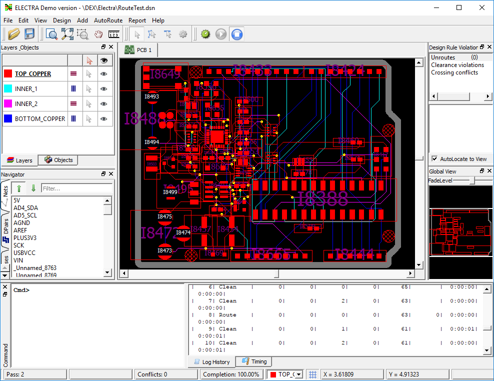
Below you can see a list of AutoTRAX DEX electrical layer by name at the upper left. The name are capitalized due to limitation in Electra.
Similarly, below the layer names you will see a list of AutoTRAX DEX net names. Again the name are capitalized due to limitation in Electra. If AutoTRAX DEX net name is not set you will see it as _UNNAMED_<XXXX> where XXXX is a unique numeric identifier. Clock on the net name to see it in the Electra viewport.
The Electra routed nets have the same color as in AutoTRAX DEX.