You set the margin or solder-mask expansion in the Solder Mask properties in the Layers panel. The margin is the gap between the pad and the solder mask. A value of 2-4 mils is usual.
The reason you have a margin > 0 is that during manufacture the layers never match up perfectly. The actual hole in the solder mask may be slightly less than what you specified, and that hole is always be placed in a slightly different location than what you specified. If your solder mask expansion is too small, then these misalignments cause the solder mask to partially or completely overlap SMT pads and through-hole pads.
With some designs, you want to make sure that the solder mask never overlaps SMD pads. This is especially critical with QFN or LGA packages where the contacts of the parts do not stick out over the plastic molding or with parts that have a very fine pitch: Even small registration issues would cause the solderable areas of the pads to be reduced.
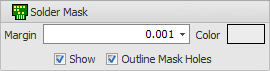
The solder mask properties
Below is a 100 Mil diameter pad with 3 different margins.
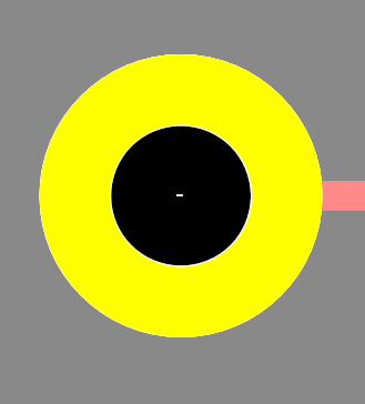
No margin
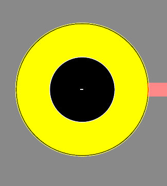
1 mil margin
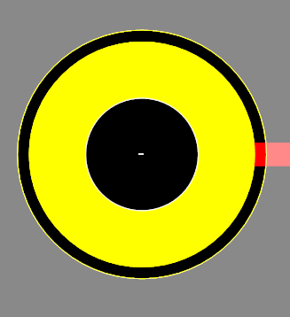
5 mil margin
Below is what happens if the solder-mask is misaligned. (Solder mask set to blue). So, the margin is to allow for manufacturing error and to ensure that all of the pad will have solder.

Perfect

Misaligned but acceptable

Misaligned and not acceptable
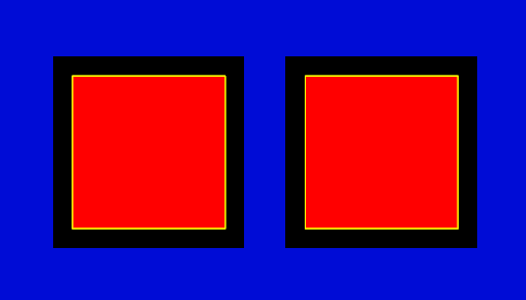
However, you do not want to make the margin too large because it could remove the solder mask between pad and risk solder bridging.
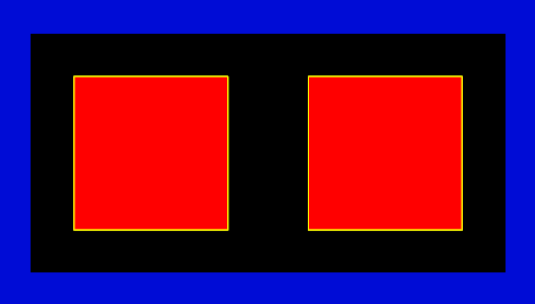
OK
Margin too large. No solder mask between pads.