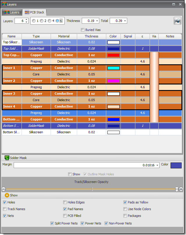
Printed circuits and footprints both contain the following layers.

The Layers Stack Panel
Document
the document layer contains graphics that you can add to document your design. There are no restrictions on color and style etc
Net
the net layer displays unrouted track segments.
If a footprint is placed outside the PCB area and the footprint net does not connect to any footprints inside the PCB area then the net that connect to the footprint will not appear. This is to avoid clutter. However when you move the footprint that is outside the PCB area the nets will be displayed.
Top Package
the top package layer contains graphics that define the 3-D content on the top of the PCB/footprint.
Top Silkscreen
the top silk screen layer defines the graphics that will be used to print a graphics design on the top of the PCB.
Top Copper
The top copper is used to define the copper tracks, but shapes, copper filled regions etc. that will be on the underside of the PCB.
Inner Layers
PCBs can also have a number of inner layers.
Bottom Copper
The bottom copper is used to define the copper tracks, but shapes, copper filled regions etc. that will be on the underside of the PCB.
Bottom Silkscreen
The top silk screen layer defines the graphics that will be used to print a graphics design on the top of the PCB.
Bottom Package
The bottom package layer contains graphics that define the 3-D content on the underside of the PCB/footprint.
Background
The background can be used for graphics that you want to be displayed underneath all the other layers. It is useful for adding objects such as images that you want to use as a trace pattern.
PCB LAYERS
Printed Circuit Boards (PCBs) can have multiple layers, each serving specific purposes to create complex and reliable circuits. The layers are generally classified into the following types:
Substrate (Base Material)
•The substrate is the foundation of a PCB, providing mechanical support. It’s typically made of materials like FR-4 (a flame-retardant fiberglass), polyimide, or other composites, depending on the application's thermal, electrical, and mechanical requirements.
•Thickness and material choice of the substrate influence the rigidity and durability of the PCB.
Copper Layer
•A thin layer of copper foil is applied to one or both sides of the PCB substrate. Each copper layer represents the electrical circuitry and connections.
•PCBs can have multiple copper layers, ranging from a single-layer PCB (one copper layer) to multi-layer PCBs (with several copper layers separated by insulation).
•The thickness of the copper is measured in ounces per square foot, where 1 oz. is a common thickness.
Solder Mask Layer
•The solder mask is a protective layer applied over the copper traces to prevent short circuits, oxidation, and solder bridges during component soldering.
•It gives the PCB its characteristic green (or sometimes red, blue, etc.) color.
•Openings in the solder mask layer expose the copper pads, allowing for component soldering.
Silkscreen Layer
•The silkscreen layer is used to apply markings, symbols, and text onto the PCB, aiding in component placement and troubleshooting.
•Typically applied in white, the silkscreen shows component designators, part numbers, and other identifiers.
Prepreg and Core (Dielectric Layers)
•Prepreg is a fiberglass material pre-impregnated with resin. It serves as an insulating layer between copper layers.
•Core is a fully cured prepreg layer with copper on both sides, used as the central dielectric layer in multi-layer PCBs.
Copper Planes (Power and Ground Layers)
For multi-layer PCBs, specific internal layers may be designated as power or ground planes, providing low-impedance paths for power distribution and signal return.
Protective Coating/Finish
•For multi-layer PCBs, specific internal layers may be designated as power or ground planes, providing low-impedance paths for power distribution and signal return.
•To prevent oxidation and ensure good solderability, the exposed copper pads are coated with finishes like HASL (Hot Air Solder Leveling), ENIG (Electroless Nickel Immersion Gold), OSP (Organic Solderability Preservative), or immersion silver.
PCB Layer Configurations
The most common configurations based on the number of layers include:
•: One layer of copper on one side of the substrate.
•: Copper layers on both sides of the substrate.
•: More than two copper layers separated by insulating material, commonly used in complex designs with dense circuitry.
Each additional layer adds complexity, cost, and functionality to the PCB, allowing for more compact designs with improved performance.