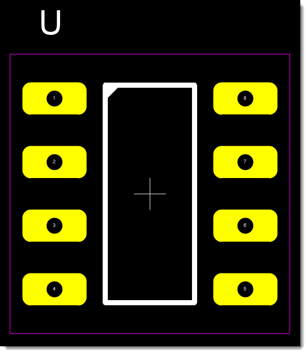
PCB Footprints (also known as land patterns or component footprints) are graphical representations of the physical layout of electronic components on a printed circuit board (PCB). A footprint defines the geometry, dimensions, and placement of pads, holes, and other features needed for mounting and connecting a specific component on the PCB.

A Footprint

PCB Footprint

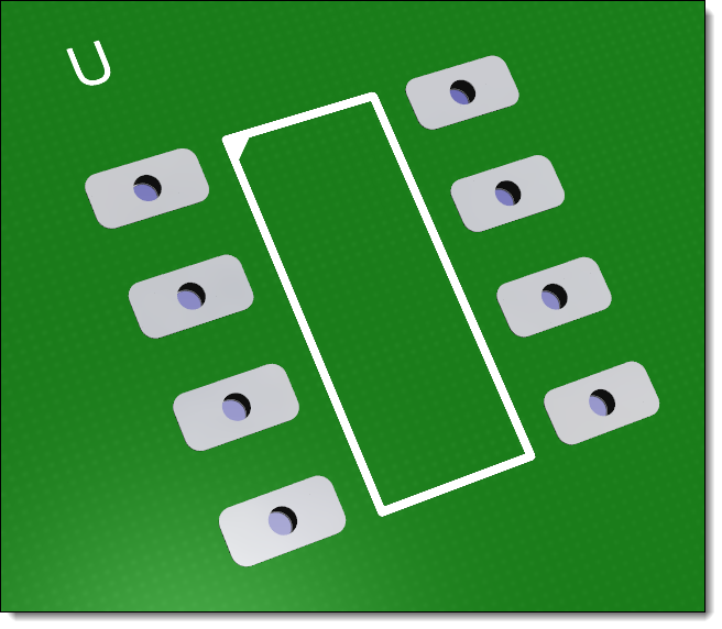
Footprint in 3D

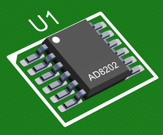
The Part for the Footprint
Components of a PCB Footprint
A typical PCB footprint includes the following elements:
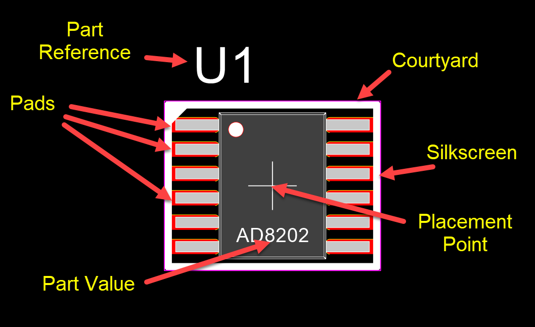
Conductive areas where component leads or pins are soldered to the PCB. For through-hole components, these include holes, while for surface-mount components, they are flat pads on the PCB surface.
The Footprint Part Reference on a PCB is a label or identifier that associates a specific physical component with its corresponding schematic symbol and footprint.
Footprint Part Values refer to the labels that represent the specific electrical or mechanical characteristics of a component on a PCB, such as resistance, capacitance, or other properties.
The Placement Point (also known as the Pick-and-Place Point or Component Origin) is a specific reference point on a component’s footprint used for positioning during the PCB assembly process.
An imaginary boundary around the component footprint that defines the minimum required space for proper placement and assembly without interference from adjacent components. It helps ensure adequate spacing for pick-and-place machines and soldering tools.
Visual labels and outlines drawn on the PCB’s silkscreen layer. They indicate component boundaries, reference designators (e.g., R1 for a resistor), polarity (for diodes, capacitors), and orientation.
Footprint Fiducials are small reference markers or alignment points included in the design of a PCB’s footprint to aid automated assembly machines, such as pick-and-place equipment or optical inspection systems.
Overall, PCB footprints are a crucial part of the PCB design process, ensuring that electronic components are correctly positioned, mounted, and connected on the circuit board, leading to reliable and functional designs.