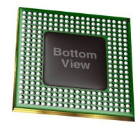
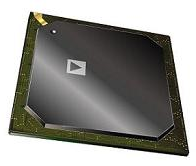
A ball grid array (BGA) is a type of surface-mount packaging used for integrated circuits. BGA packages are used to permanently mount devices such as microprocessors. A BGA can provide more interconnection pins than can be put on a dual in-line or flat package. The whole bottom surface of the device can be used, instead of just the perimeter. The leads are also on average shorter than with a perimeter-only type, leading to better performance at high speeds.
 Soldering of BGA devices requires precise control and is usually done by automated processes. A BGA device is never mounted in a socket in use.
Advantages
The BGA is descended from the pin grid array (PGA), which is a package with one face covered (or partly covered) with pins in a grid pattern. These pins conduct electrical signals from the integrated circuit to the printed circuit board (PCB) on which it is placed. In a BGA, the pins are replaced by balls of solder stuck to the bottom of the package. These solder spheres can be placed manually or with automated equipment. The solder spheres are held in place with a tacky flux until soldering occurs. The device is placed on a PCB with copper pads in a pattern that matches the solder balls. The assembly is then heated, either in a reflow oven or by an infrared heater, causing the solder balls to melt. Surface tension causes the molten solder to hold the package in alignment with the circuit board, at the correct separation distance, while the solder cools and solidifies.
The BGA is a solution to the problem of producing a miniature package for an integrated circuit with many hundreds of pins. Pin grid arrays and dual-in-line surface mount (SOIC) packages were being produced with more and more pins, and with decreasing spacing between the pins, but this was causing difficulties for the soldering process. As package pins got closer together, the danger of accidentally bridging adjacent pins with solder grew. BGAs do not have this problem when the solder is factory-applied to the package.
A further advantage of BGA packages over packages with discrete leads (i.e. packages with legs) is the lower thermal resistance between the package and the PCB. This allows heat generated by the integrated circuit inside the package to flow more easily to the PCB, preventing the chip from overheating.
 The shorter an electrical conductor, the lower its inductance, a property which causes unwanted distortion of signals in high-speed electronic circuits. BGAs, with their very short distance between the package and the PCB, have low inductances and therefore have far superior electrical performance to leaded devices.
Disadvantages
A disadvantage of BGAs is that the solder balls cannot flex in the way that longer leads can, so they are not compliant. As with all surface mount devices, bending due to a difference in coefficient of thermal expansion between PCB substrate and BGA (thermal stress) or flexing and vibration (mechanical stress) can cause the solder joints to fracture.
Thermal expansion issues can be overcome by matching the mechanical and thermal characteristics of the PCB to those of the package. Typically, plastic BGA devices more closely match PCB thermal characteristics than ceramic devices.
The predominant use of RoHS compatible lead-free solder alloy assemblies have presented some further challenges to BGAs including "head in pillow" soldering phenomenon, "pad cratering" problems as well as their decreased reliability versus lead-based solder BGAs in extreme operating conditions such as high temperature, high thermal shock and high gravitational force environments, in part due to lower ductility of RoHS-compliant solders.
Mechanical stress issues can be overcome by bonding the devices to the board through a process called "under filling", which injects an epoxy mixture under the device after it is soldered to the PCB, effectively gluing the BGA device to the PCB. There are several types of under fill materials in use with differing properties relative to workability and thermal transfer. An additional advantage of under fill is that it limits tin whisker growth.
Another solution to non-compliant leads is to put a "compliant layer" in the package that allows the balls to physically move in relation to the package. This technique has become standard for packaging DRAMs in BGA packages.
Once the package is soldered down, it may be difficult to look for soldering faults. X-ray machines, Industrial CT Scanning machines, special microscopes as well as endoscopes to look underneath the soldered package have been developed to overcome this problem. If a BGA is found to be badly soldered, it can be removed in a rework station, which is a jig fitted with infrared lamp (or hot air), a thermocouple and a vacuum device for lifting the package. The BGA can be replaced with a new one, or the BGA can be refurbished (or reballed) and re-installed on the circuit board. Pre-configured solder balls matching the array pattern (preforms) can be used to reballing the BGA's when only one or a few need to be reworked.
Due to cost of X-ray BGA inspection, electrical testing is very often used. Very common is boundary scan testing using IEEE 1149.1 JTAG port.
During development it is not practical to solder BGAs into place, and sockets are used instead, but tend to be unreliable. There are two common types of socket: the more reliable type has spring pins that push up under the balls, although it does not allow using BGAs with the balls removed as the spring pins may be too short.
The less reliable type is a ZIF socket, with spring pinchers that grab the balls. This does not work well, especially if the balls are small.
Expensive equipment is required to reliably solder BGA packages; hand-soldering BGA packages is very difficult and unreliable, usable only for the smallest packages in the smallest quantities.
Other BGA package types
CABGA Chip Array Ball Grid Array
CBGA and PBGA denote the Ceramic or Plastic substrate material to which the array is attached.
CTBGA Thin Chip Array Ball Grid Array
CVBGA Very Thin Chip Array Ball Grid Array
DSBGA Die-Size Ball Grid Array
FBGA or Fine Ball Grid Array based on ball grid array technology. It has thinner contacts and is mainly used in system-on-a-chip designs. Known as FineLine BGA by Altera.
FCmBGA Flip Chip Molded Ball Grid Array
LBGA Low-profile Ball Grid Array
LFBGA Low-profile Fine-pitch Ball Grid Array
MBGA Micro Ball Grid Array
MCM-PBGA Multi-Chip Module Plastic Ball Grid Array
PBGA Plastic Ball Grid Array
SuperBGA (SBGA) Super Ball Grid Array
TABGA Tape Array BGA
TBGA Thin BGA
TEPBGA Thermally Enhanced Plastic Ball Grid Array
TFBGA or Thin and Fine Ball Grid Array
UFBGA and UBGA and Ultra Fine Ball Grid Array based on pitch ball grid array