PCB component placement refers to the process of arranging electronic components on a printed circuit board (PCB). It involves determining the optimal positions for each component to ensure proper functionality, efficient routing of traces, and ease of manufacturing and assembly. Here's an overview of PCB component placement:
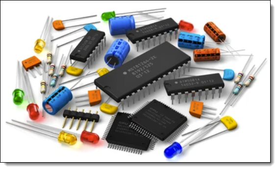
Component Selection
Before placement, you need to select the appropriate components for your circuit based on the design requirements. Consider factors such as component type, package size, electrical characteristics, and availability.

Component Selection
Schematic-Based Placement
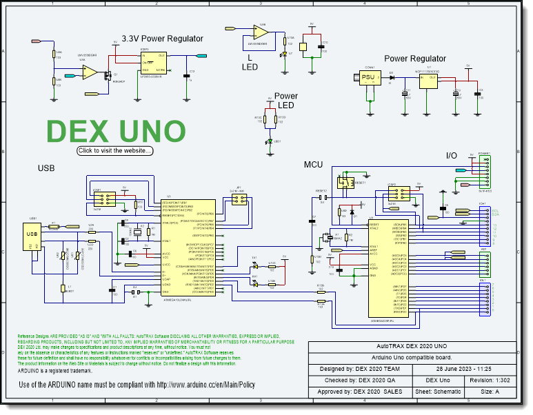
Component placement is typically based on the schematic diagram of the circuit. The schematic provides the interconnections between components, allowing you to understand the relationships and dependencies between them.

Schematic-Based Placement
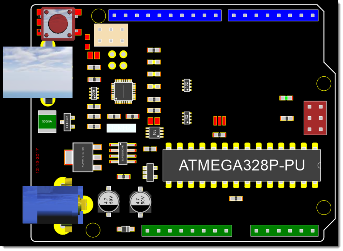
Component Positioning
Consider the following factors when positioning components on the PCB:
•Functional Requirements: Arrange the components to meet the functional requirements of the circuit. Group related components together and position them in a logical and intuitive manner.
•Signal Integrity: Place components to minimize signal degradation and optimize signal integrity. Consider factors such as trace length, impedance matching, and minimizing signal crosstalk or noise.
•Thermal Considerations: Consider thermal requirements of the components. Place heat-generating components, such as power devices or ICs, in locations that allow for efficient heat dissipation. Avoid placing heat-sensitive components near heat sources.
•Mechanical Constraints: Account for any mechanical constraints, such as the size and shape of the enclosure or system where the PCB will be installed. Ensure that the component placement fits within the available space and allows for proper assembly and maintenance.
•Assembly and Manufacturing: Position components in a way that facilitates efficient assembly and manufacturing processes. Consider factors such as access for soldering, test point placement, and avoidance of overcrowding that may impede assembly or inspection.

PCB Component Positioning
Component Orientation
Determine the appropriate orientation of components. Consider factors such as pin configurations, polarized components (e.g., diodes or capacitors), and alignment with reference designators and silkscreen markings.
Design Iteration
PCB component placement often involves an iterative process. You may need to revise and optimize the placement based on factors such as signal routing constraints, manufacturability issues, or design rule violations.

PCB Design Iterations
PCB Design Software
Use PCB design software tools that offer features to assist with component placement. These tools often provide automated or manual placement capabilities, design rule checks, and visualization tools to aid in component positioning and optimization.
It's important to strike a balance between functional requirements, signal integrity, thermal considerations, mechanical constraints, and manufacturing efficiency when placing components on a PCB. Consider consulting with experienced PCB designers or engineers and utilizing appropriate software tools to ensure an effective and optimized component placement.

Find out more...