All via to PCB border spacings that are less than the minimum via to PCB border clearance will be marked as shown below.
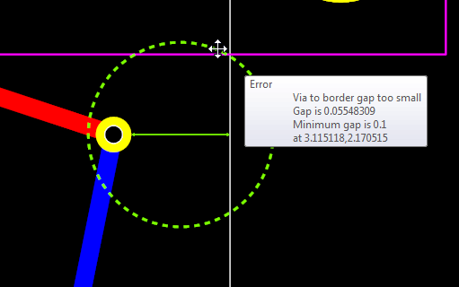
Via too close to the PCB border - marked with green circle and line segment showing the distance (and arrow if error selected)
|
<< Click to Display Table of Contents >> Navigation: Designing a PCB > Projects > The PCB > Checking Your PCB Design > Via to Border Clearance |
All via to PCB border spacings that are less than the minimum via to PCB border clearance will be marked as shown below.
Via too close to the PCB border - marked with green circle and line segment showing the distance (and arrow if error selected)