When generating Gerber files, AutoTRAX DEX will automatically generate up to 2 additional file for the top and bottom layer solder paste stencils, but only if there are SMT pads on the top or bottom side. You can optionally add solder mask areas to no mask areas and also add your own custom no mask shapes. No file is generated for a side if there are Solder paste areas on that side.
No holes are output for TPH pads.
The 2 files with a (.gbr) extension are called:
•Top Solder Paste
•Bottom Solder Paste
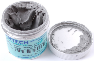 Solder paste (or solder cream) is used to connect the leads of surface mount integrated chip packages to attachment points (pads/lands) in the circuit patterns on a printed circuit board. The paste is typically applied to the pads using a stencil to "print" the paste, although other methods, like dispensing from a tube, are also used.
A majority of the defects in circuit-board assembly are caused due to issues in the solder-paste printing process or due to defects in the solder paste. There are many different types of defects—too much solder, and the solder melts and connects too many wires (bridging), resulting in a short circuit. Insufficient amounts of paste result in incomplete circuits. Head-in-pillow defects, or incomplete coalescence of ball grid array (BGA) sphere and solder paste deposit, is a failure mode that has seen increased frequency since the transition to lead-free soldering. Often missed during inspection, a head-in-pillow (HIP) defect appears like a small head resting on a pillow with a visible separation in the solder joint at the interface of the BGA sphere and paste deposit. An electronics manufacturer needs experience with the printing process, specifically the paste characteristics, to avoid costly re-work on the assemblies. The paste's physical characteristics, like viscosity and flux levels, need to be monitored periodically by performing in-house tests.
Solder paste is typically used in a screen-printing process, in which paste is deposited over a stainless steel or polyester mask to create the desired pattern on a printed circuit board. The paste may be dispensed pneumatically, by pin transfer (where a grid of pins is dipped in solder paste and then applied to the board), or by jet printing (where the paste is sprayed on the pads through nozzles, like an ink-jet printer).
As well as forming the solder joint itself, the paste carrier/flux must have sufficient tackiness to hold the components while the assembly passes through the various manufacturing processes, perhaps moved around the factory.
Printing is followed by preheating and reflow (melting).
The paste manufacturer will suggest a suitable reflow temperature profile to suit their individual paste; however, one can expend too much energy on this. The main requirement is a gentle rise in temperature to prevent explosive expansion ("solder balling"), yet activate the flux. Thereafter, the solder melts. The time in this area is known as Time Above Liquidus. A reasonably rapid cool-down period is required after this time.
A good tin/lead solder joint will be shiny and relatively concave. This will be less so with lead-free solders.
As with all fluxes used in electronics, residues left behind may be harmful to the circuit, and standards (e.g., J-std, JIS, IPC) exist to measure the safety of the residues left behind.
In most countries, "no-clean" solder pastes are the most common; in the United States, water-soluble pastes (which have compulsory cleaning requirements) are common.