PCB plotting refers to the process of creating a physical layout or design from a conceptual electronic design as part of the PCB manufacturing process. This is a critical step where the digital blueprint becomes the guide for the actual board that will be produced. Here’s a deeper dive into what PCB plotting involves and why it’s important.
Understanding PCB Plotting
•From Schematic to Design: Before plotting begins, the PCB design is conceptualized in a schematic. Engineers then use electronic design automation (EDA) software to translate these schematics into a digital model of the PCB, including all layers, copper traces, vias, and components. This digital model is what will be 'plotted' onto the physical board.
•Gerber Files: The industry-standard format for PCB design files is "Gerber" format. These files contain all the necessary information for the PCB's layers and are used by the manufacturing machines. Each layer (copper, solder mask, silkscreen, etc.) will have its own file, and these files act as the 'maps' for plotting the PCB design onto the physical layers.
•Plotting Process: The term "plotting" comes from older processes where a plotter (a large, specialized printer) was used to create a highly accurate, to-scale print of each PCB layer on a transparent sheet. These sheets (photo masks) were then used in the photo-lithographic PCB manufacturing process, where they helped transfer the design onto the copper layers. Although technology has evolved, the term persists and now refers more generally to the generation of manufacturing instructions/guidelines from digital designs.
•Modern Photoplotting: Today, the process is more direct. Advanced machines use the information in the Gerber files to directly image the PCB design onto the board layers, often using lasers that are far more accurate than older physical plotters. This allows for the incredibly precise transfer of even the most complex and miniaturized designs onto a physical substrate.
•Inspection and Quality Control: After plotting, the PCBs go through rigorous inspection. Automated Optical Inspection (AOI) is a key part of quality control, ensuring that the layout has been accurately rendered onto the PCB and that there are no defects, like short circuits or missing components, which could cause failures.
Importance of Accurate PCB Plotting
•Fidelity to Design: The plotting process must be extremely accurate to ensure the final PCB precisely matches the original digital design. Mistakes in plotting can lead to short circuits, breaks, or non-functional boards, especially in complex, multi-layer PCBs.
•Reliability and Functionality: Accurate plotting is crucial for the reliability of the PCBs, especially for those used in critical applications like medical devices, aerospace, and automotive systems, where a malfunction could be catastrophic.
•Cost Efficiency: Errors in the plotting process can result in the need for redesigns or re-manufacturing, both of which lead to additional costs and delays. Accurate plotting helps in reducing wastage and improving production efficiency.
In conclusion, PCB plotting is a technical and precise process that plays a critical role in electronics manufacturing. With advancements in technology, especially in direct laser imaging and other forms of photoplotting, this process has become faster and more accurate, catering to the needs of modern electronics that often require incredibly detailed and reliable PCBs.
To plot your PCB click the Tools→CAM→ button.
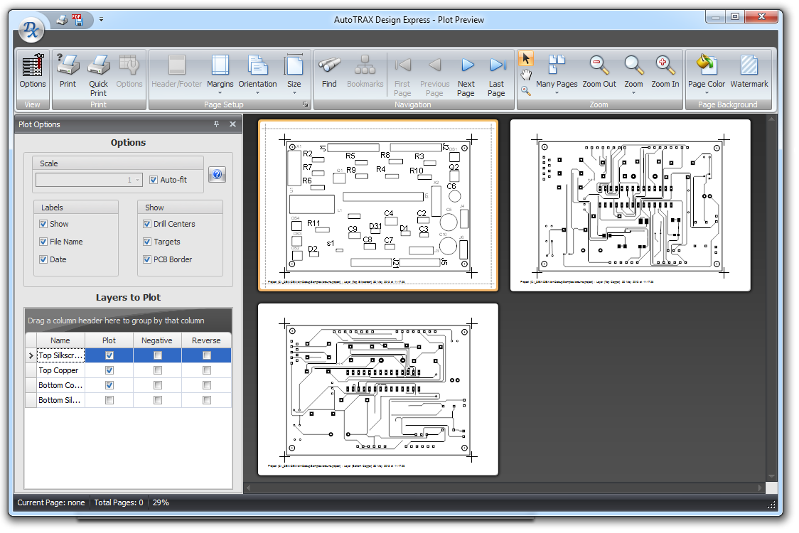
Plot Preview
The ploy preview shown above consists of a ribbon menu, a options panel on the left and a preview window to the right of the options panel and below the ribbon menu.
click  to print the selected pages.
Ribbon Menu
The ribbon menu can be split into 2 parts, the View button group on the left and the common ribbon button groups on the right.
The  button shows/hides the option panel shown below.
Click to read about the Common Print Menu
The Option Panel
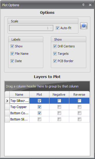
Options Dialog
The options panel lets you scale the printing or have the sheets automatically fill the printed page.
Scale
Check  to have the sheets automatically fill the printed page, If you uncheck it, you can set the print scale. Note, it is possible to set the scale such that the sheet will not all fit on the printed page.
Labels
 Check to print plot layer labels
  Check to add a the file name to each plot.
  Check to add a date to each plot.
 Show
 Check add small drill target/centers to each pad/via that has a hole.
 Check to add targets to the printed output.
 Check to include the PCB border in the printed output.
Layers to Plot
Check/uncheck the check boxes in the Plot column to include/exclude the layer in the print run.
Check/uncheck the check boxes in the Negative column to print that sheet in negative.
Check/uncheck the check boxes in the Reverse column to print that sheet reversed in the horizontal direction.
Clicking  displays this help topic.