A fiducial marker or fiducial is an object placed in the field of view of an imaging system which appears in the image produced, for use as a point of reference or a measure. It may be either something placed into or on the imaging subject, or a mark or set of marks in the reticule of an optical instrument.
A fiducial mark is a printed board artwork feature that is created in the same process as the conductive pattern and that of is a measurable point for component mounting with respect to a land pattern or land patterns.
A PCB fiducial is a circular area of copper on either the top of the bottom side of the PCB that is used for Alignment using optical recognition systems. The fiducial mark and this PCB copper tracks must be etched in the same step to ensure alignment.

A PCB fiducial in the 2D View
A PCB fiducial in the 3D View
A fiducial marks is made up of 3 parts.
1.A solid circle of copper on the top or bottom copper layer. This is the alignment target.
2.An opening in the solder mask so the circular alignment target is clearly visible.
3.An option text label to the side of the opening in the solder mask
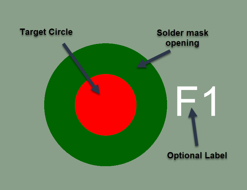
A Fiducial Mark
The fiducial marks provide a common set of data points for all steps in the PCB assembly process. This allows all pieces of equipment used for assembly to accurately locate the parts based on the circuit pattern.
In printed circuit board (PCB) manufacturing, fiducial marks, also known as circuit pattern recognition marks, allow SMT placement equipment to accurately locate and place parts on boards. These devices locate the circuit pattern by providing common measurable points. They are usually made by leaving a circular area of the board bare from solder-mask coating. Inside this area is a circle exposing the copper plating beneath. This center metallic disc can be solder-coated, gold-plated or otherwise treated, although bare copper is most common if not a current-carrying contact. Alternatively, it is possible to use clear solder-mask lacquer to cover the fiducials. In order to minimize rounding errors it was good practice to place fiducials in the same grid (or some multiple of it) that was used to place the parts, however, this isn't always possible on high-density boards nor is it a requirement any more with modern high-precision machines.
Most placement machines are fed boards for assembly by a rail conveyor, with the board being clamped down in the assembly area of the machine. Each board will clamp slightly differently than the others, and the variance—which will generally be only tenths of a millimeter—is sufficient to ruin a board without proper calibration. Consequently, a typical PCB will have multiple fiducials to allow placement robots to precisely determine the board's orientation. By measuring the location of the fiducials relative to the board plan stored in the machine's memory, the machine can reliably compute the degree to which parts must be moved relative to the plan, called offset, to ensure accurate placement.
Using three fiducials enables the machine to determine PCB offset in both the X and Y axes, as well as to determine if the board has rotated during clamping, allowing the machine to rotate parts to be placed to match. Such fiducials are also called global fiducials. Global fiducials are also used in conjunction with stencil printing. Without them the printer would not print the solder paste in exact alignment with the pads. Parts requiring a very high degree of placement precision, such as ball grid array packages, may have additional local fiducials near the package placement area of the board to further fine-tune the targeting. Local fiducial, however, cannot be used in the stencil printing process.
Conversely, low end, low-precision boards may only have two fiducials, or use fiducials applied as part of the screen printing process applied to most circuit boards. Some very low-end boards may use the plated mounting screw holes as ersatz fiducials, although this yields very low accuracy.
For prototyping and small batch production runs, the use of a fiducial camera can greatly improve the process of board fabrication. By automatically locating fiducial markers, the camera automates board alignment. This helps with front to back and multilayer applications, eliminating the need for set pins.
There are 3 types of fiducial marks. These are panel fiducials, global fiducials and local fiducials.
Panel fiducials are used on board panels where 2 are more PCBs are manufactured together.
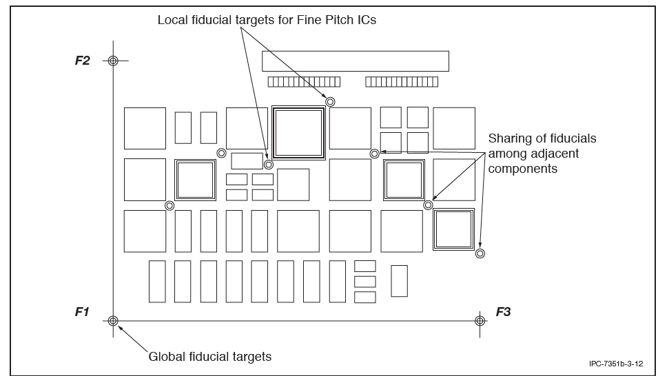
PCB with global and local fiducials.
Global Fiducials
Global fiducials are used to locate the position of all circuit features on an individual PCB. When multiple PCBs are created on the same PCB panel then these global fiducials are referred to as panel fiducials.
A minimum of three fiducial panel/global marks are required for correction of offsets (X, Y positions), rotational offsets (angle position). These should be located orthogonally as far as possible on the PCB panel.
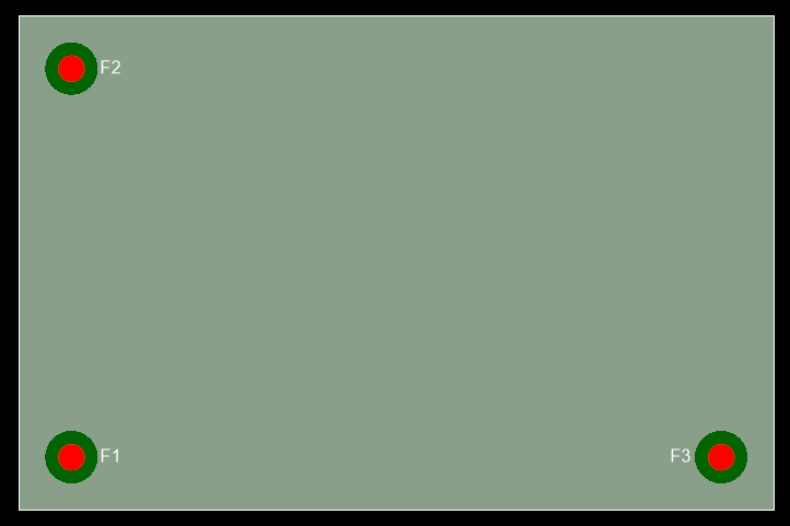
Very small PCB with 3 global fiducials F1, F2 and F3
It is good practice to locate global fiducials in a three point grade are shown below. The first fiducial is located at the lower left usually at the Norton – not location. The second and third fiducials are located vertically or horizontally aligned to the first fiducial. These fiducials should be located on both the top and bottom layers of your PCB that contains surface mount as well as through all components since even so all assemblies systems are beginning to utilize visual alignment systems.
Local Fiducials
Local fiducial marks are used to locate the position of an individual component requiring more precise placement.
For these components, 2 local fiducial marks are required for correction of translational offsets (X and Y position) and rotational offsets (θ position ). This can be to marks located directly opposite each other within the outside perimeter of the land pattern.
All fine pitch components should have 2 local fiducial marks designed into the footprint to ensure that enough fiducials are available every time a component is placed, removed and/ or replaced on the PCB. Fiducial must have a solder mask opening large enough to keep the optical target absolutely free of solder mask. If solder mask should get into the optical target area them some vision alignment systems may fail due to insufficient contrast in the target.
If space is limited, you may be able to share fiducial from adjacent component within the local constraint. Also, in such a space limited situation and the PCB is deemed by your manufacturer to be sufficiently small, component fiducials can be omitted and global fiducials used in their place.
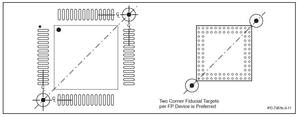
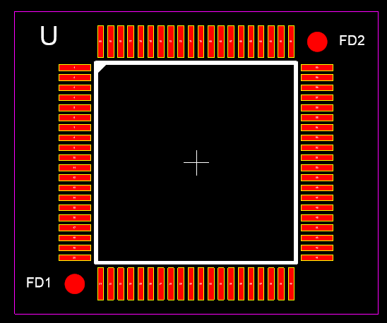
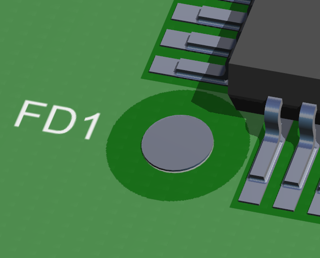
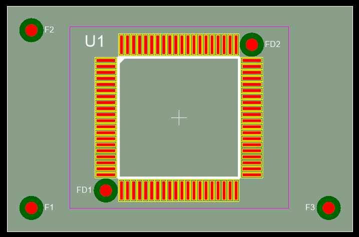
QFP with 2 corner local fiducials (FD1 and FD2)
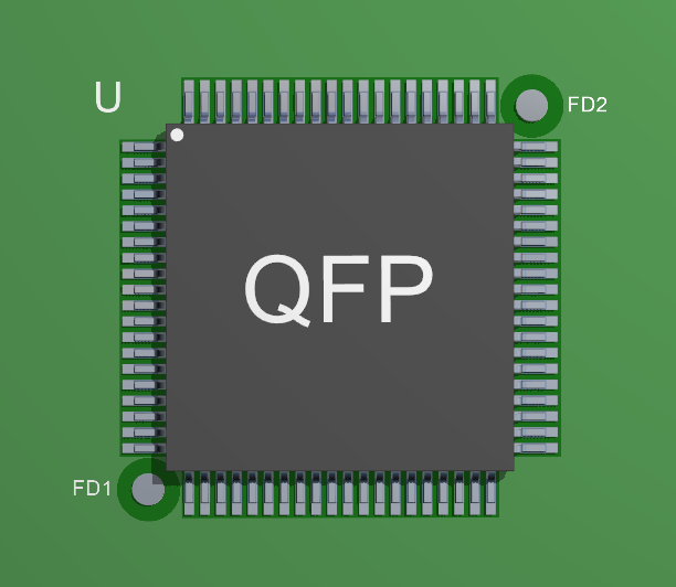
QFP with 2 corner local fiducials (FD1 and FD2)
The size and shape of fiducials
The best fiducial shape is a solid full-circle and that is what AutoTRAX DEX does. The preferred diameter of the fiducial mark is 1 mm as per the IPC – 7351B specification. You are recommended to keep the size is 1 mm although you can change it if you wish.
Fiducial marks should not vary in size on the same printer circuit board by more than 25 µm. A clear area devoid of any other circuit features are markings should exist around the fiducial mark. The minimum size of the clear area is recommended to be twice the radius of the central mark.
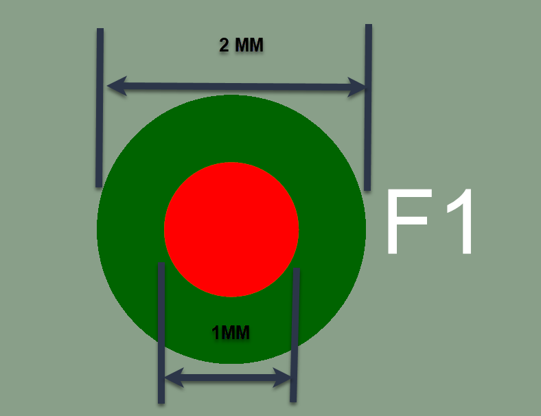
Recommended Fiducial Dimensions - IPC 7351B
Zonal fiducials
To facilitate the accurate placement of multiple SMD components that are not near component specific local fiducials are global fiducials you can place additional solo fiducial targets within an area of the PCB to compensate for PCB dimensional stability.
Material
the fiducial mark is copper which may or may not be tend. If you have a solder mask on the PCB it must not cover the fiducial mark of the clearance area. Note: that excessive oxidation of a fiducial marks copper may degrade the readability.
Edge clearance
the age of the fiducial should be no closer to the edge of the PCB than the sum of 4.75 mm and the minimum fiducial clearance required. If less then you may need to add a PCB board only fixture.
Contrast
the best performance is achieved when a consistent high contrast is present between the fiducial mark and the PCB base material.
The background of all fiducial marks must be the same.