You can set and edit the layers using the  button at the top left of the layers panel.
The layer editor dialog box shown below will appear.
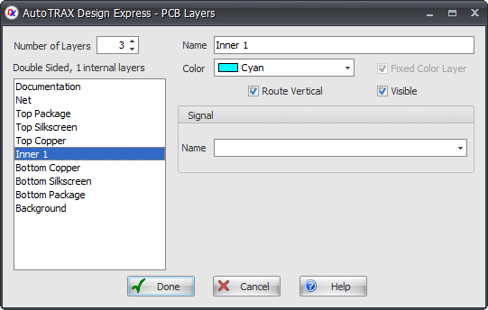
Set the number of layers using the 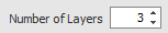 control.
To edit the properties of an individual layer first select it using the left layers list box.
Each layer can have it's own name. Se it using the  control.
All layers except the top and bottom package layers. the documentation layer, and the background layer have a fixed color. You can set the fixed color for these layers using the 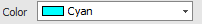 layer color control.
Check/uncheck  to set the preferred auto-routing direction of the layer. This only applies to electrical layers.
Check/uncheck  to hide/show a layer.
Signals
Layers can act as signal planes. Enter the name of the signal for the layer. If a layer has a signal name then it will be filled with copper with holes for pads and vias that do not connect to the layer.
Tracks with the same net name as the layer will connect to that layers via any pads/vias that pass through to that layer. These pads/vias will connect directly to the signal layer.
Enter the signal name in the 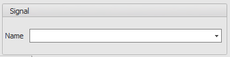 control.
Clear the signal name (set it to nothing) to make the layer act as a normal layer.