Back-drill and Controlled Depth Drilling
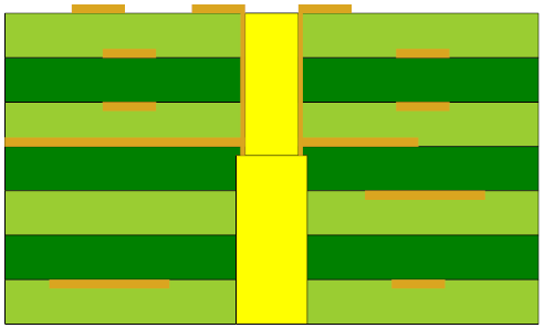 The back drill process removes stubs from plated-through-holes (vias). Stubs are the unnecessary /unused portions of vias, which extend further than the last connected inner layer.
Stubs can lead to reflections, as well as disturbances of capacity, inductance and impedance. This discontinuity errors become critical with increasing propagation speed.
Back-planes and thick Printed Circuit Boards in particular, can endure significant signal integrity disturbances through stubs. For High Frequency PCBs (e.g. with Impedance control), the application of back drilling, as well as the application of blind and buried vias, can be part of the solution.
Back-drill can be applied to any type of circuit board where stubs cause signal integrity degradation, with minimal design and layout considerations. In contrast, when using blind vias, the aspect ratio has to be kept in mind.
Advantages of Back-drill
•Reduced deterministic jitter
•Lower bit error rate (BER)
•Less signal attenuation with improved impedance matching
•Increased channel bandwidth
•Increased data rates
•Reduced EMI radiation from the stubs
•Reduced excitation of resonance modes
•Reduced via-to-via crosstalk
•Aspect ratio can be neglected (in contrast to blind vias)