PCB (Printed Circuit Board) differential pairs are a fundamental concept in high-speed digital and analog circuit design. They consist of two conductors that carry electrical signals, with equal and opposite voltage polarities. These pairs are used to transmit signals while minimizing electromagnetic interference (EMI) and noise.
Here are some key points about PCB differential pairs:
•Signal Integrity: Differential pairs are used primarily to maintain signal integrity in high-speed signal transmission. They help to reduce electromagnetic interference, crosstalk, and noise in the signal.
•Equal and Opposite Signals: In a PCB differential pair, one conductor carries the signal (the positive or non-inverted signal), while the other carries an equal but opposite version of the same signal (the negative or inverted signal).
•Balanced Transmission: The signals in a differential pair are transmitted as a balanced pair, meaning that any noise or interference affecting one conductor is likely to affect the other similarly. This allows the receiver to differentiate between the intended signal and any noise or interference.
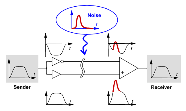
•Common Mode Rejection: One of the key advantages of using a differential pair is its ability to reject common-mode noise. Common-mode noise refers to noise that appears simultaneously on both conductors of the pair. Since the receiver of a differential pair looks at the difference between the two signals, common-mode noise tends to cancel out.
•Controlled Impedance: Differential pairs typically require controlled impedance traces on the PCB to maintain signal integrity. Proper impedance matching between the traces and the components helps to minimize signal distortion and reflections.
•Applications: Differential pairs are commonly used in high-speed data transmission interfaces such as USB, HDMI, Ethernet, and PCIe. They are also used in various communication interfaces, including LVDS (Low-Voltage Differential Signaling) and RS-485.
•Layout Considerations: Proper layout and routing of the traces are crucial for maintaining signal integrity in PCB differential pairs. The traces should be routed closely together with consistent spacing and controlled impedance.
In summary, PCB differential pairs are a critical component of high-speed digital and analog circuits, providing reliable and noise-immune transmission of signals across printed circuit boards. They are essential for modern electronic devices that require fast and reliable data communication.
Differential signaling is a method for electrically transmitting information using two complementary signals. The technique sends the same electrical signal as a differential pair of signals, each in its own conductor. The pair of conductors can be wires (typically twisted together) or traces on a circuit board. The receiving circuit responds to the electrical difference between the two signals, rather than the difference between a single wire and ground. The opposite technique is called single-ended signaling. Differential pairs are usually found on printed circuit boards, in twisted-pair and ribbon cables, and in connectors.
Differential signaling is often used in computers to reduce electromagnetic interference, because complete screening is not possible with micro-strips and chips in computers, due to geometric constraints and the fact that screening does not work at DC. If a DC power supply line and a low-voltage signal line share the same ground, the power current returning through the ground can induce a significant voltage in it. A low-resistance ground reduces this problem to some extent. A balanced pair of micro-strip lines is a convenient solution, because it does not need an additional PCB layer, as a strip line does. Because each line causes a matching image current in the ground plane, which is required anyway for supplying power, the pair looks like four lines and therefore has a shorter crosstalk distance than a simple isolated pair. In fact, it behaves as well as a twisted pair. Low crosstalk is important when many lines are packed into a small space, as on a typical PCB.
In single-ended signaling, the transmitter generates a single voltage that the receiver compares with a fixed reference voltage, both relative to a common ground connection shared by both ends. In many instances single-ended designs are not feasible. Another difficulty is the electromagnetic interference that can be generated by a single-ended signaling system that attempts to operate at high speed.
Provided that the source and receiver impedance in the differential signaling circuit are equal, external electromagnetic interference tends to affect both conductors identically. Since the receiving circuit only detects the difference between the wires, the technique resists electromagnetic noise compared to one conductor with an unpaired reference (ground). The technique works for both analog signaling, as in balanced audio—and digital signaling, as in RS-422, RS-485, Ethernet over twisted pair, PCI Express, DisplayPort, HDMI, and USB.
A differential signaling system is where a signal is transmitted down a pair of tightly coupled tracks with one of these carrying the signal and the other carrying an equal but opposite image of the signal. Differential signaling was developed to resolve situations where the logic reference ground of the signal source could not be well connected to the logic reference ground of the load. Differential signaling is inherently immune to common mode electrical noise, the most common interference artifact present in an electronic product. Differential signaling also minimizes electromagnetic interference (EMI) generated from the signal on the PCB.
The electronics industry, particularly in portable and mobile devices, continually strives to lower supply voltage to save power and reduce emitted electromagnetic radiation. A low supply voltage, however, reduces noise immunity. Differential signaling helps to reduce these problems because, for a given supply voltage, it provides twice the noise immunity of a single-ended system.
To see why, consider a single-ended digital system with supply voltage Vs. The high logic level is Vs, and the low logic level is 0 V. The difference between the two levels is therefore Vs-0 = Vs.
Now consider a differential system with the same supply voltage. The voltage difference in the high state, where one wire is at Vs , and the other at 0 V, is Vs-0 = Vs. The voltage difference in the low state, where the voltages on the wires are exchanged, is 0-Vs = -Vs The difference between high and low logic levels is therefore Vs-(-Vs) = 2Vs,. This is twice the difference of the single-ended system. If the voltage noise on one wire is uncorrelated to the noise on the other one, it takes twice as much noise to cause an error with the differential system as with the single-ended system. In other words, differential signaling doubles the noise immunity.
The technique minimizes electronic crosstalk and electromagnetic interference, both noise emission and noise acceptance, and can achieve a constant or known characteristic impedance, allowing impedance matching techniques important in a high-speed signal transmission line or high quality balanced line and balanced circuit audio signal path.
Resistance to electromagnetic interference
This advantage is not directly due to differential signaling itself, but to the common practice of transmitting differential signals on balanced lines. Single-ended signals are still resistant to interference if the lines are balanced and terminated by a differential amplifier.
Electra
You create differential pairs in the schematic, not in the PCB. The PCB nets will be automatically used to differential pair status.
Differential pair routing process starts by identifying gather points at the proximity of the fan out vias. The main part of the connections are then auto-routed between the gather points. The auto router applies the same multi pass conflict reduction strategy to the differential pair nets and length constrained nets in order to reach the highest completion rate.
No T-junction or vias are used during routing of the differential pairs.
45 degree routing style can be predefined for the differential pair routing.
Differential pairs are treated as signal nets and take part into the adaptive auto-routing strategy with conflict resolution.