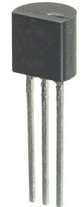
 The TO-92 is a widely used style of semiconductor package mainly used for transistors. The case is often made of epoxy or plastic, and offers compact size at a very low cost. The JEDEC TO-92 descriptor is derived from the original full name for the package: Transistor Outline Package, Case Style 92.
Today, the industry prefers the new TO-226 nomenclature for the TO-92 three-leaded enclosure.
There are three TO-206 variants: TO-206AA with three straight leads; TO-206AB with the lead 2 formed to create a triangular pattern between the leads and the TO-206AC with the lead 2 omitted. (the latter is in fact a diode package and is mainly used for Varactor tuning diodes and shunt voltage references).
Construction and orientation
The case is molded around the transistor elements in two parts; the face is flat, bearing a machine-printed part number. The back is semi-circularly-shaped. A line of molding flash from the injection-molding process can be seen around the case.
The leads protrude from the bottom of the case. When looking at the face of the transistor, the leads are commonly configured from left-to-right as the emitter, base, and collector for 2N series (JEDEC) transistors, however, other configurations are possible, such as emitter, collector, and base commonly used for 2S series (Japanese) transistors.
If the face has a part name made up of only one letter and a few numbers, it is usually assumed to be a Japanese part number (with the base on the end rather than in the center). Thus, "C1234" would likely be a 2SC1234 device.
The leads coming out of the case are spaced 0.05" (1.27 mm) apart. It is often convenient to bend them outward to a 0.10" (2.54 mm) spacing to make more room for wiring. Units with their leads pre-bent may be ordered to fit specific board layouts, depending on the application. Otherwise, the leads may be bent manually; however, care must be taken as they can break easily.
The physical dimensions of the TO-92 housing may vary sightly depending of the manufacturer, however, the 1.27mm lead spacing must be respected.
Advantages
•Transistors of this type can be made very inexpensively and take up very little board space. Most models are readily available in large quantities from wholesale distributors.
•They are easy to find in small electronics stores because of their wide usefulness, making them a popular choice for hobby work and prototyping.
Disadvantages
The main disadvantage of this style of case is the lack of heat sinking.
•Transistors and ICs of these types cannot handle as much power as higher-power equivalents, such as the TO-220 and can burn out quickly if they dissipate excessive power.
•There is no standard pin-out for the TO-92. The American BJT's use the E-B-C pin-out while their Japanese counterparts use the E-C-B pin-out and some RF devices use the B-E-C pin-out.
More often than not, however, the disadvantages concerning accidental destruction are greatly outweighed by the small size and low cost of producing these units.
Although TO-92 devices are mainly used in low-voltage / low-current (<30 V; <1 A) applications, high-voltage (600 Volt Vce) and high-current (5 A Ic) devices are available. Nominal maximum power dissipation is less than one watt (600 mW).