A small-outline integrated circuit (SOIC) is a surface-mounted integrated circuit (IC) package which occupies an area about 30–50% less than an equivalent DIP, with a typical thickness that is 70% less. They are generally available in the same pin-outs as their counterpart DIP ICs. The convention for naming the package is SOIC or sometimes just SO followed by the number of pins. For example, a 14-pin 4011 would be housed in an SOIC-14 or SO-14 package.
Small-outline J-leaded package (SOJ) is a version of SOIC with J-type leads instead of gull-wing leads.
JEDEC and EIAJ standards
SOIC actually refers to at least two different package standards. The EIAJ SOIC body is approximately 5.3 mm (0.21 in) wide while the JEDEC SOIC body is approximately 3.8 mm (0.15 in) wide. The EIAJ packages are also thicker and slightly longer. Otherwise the packages are similar.
Note that because of this, SOIC is not specific enough of a term to describe parts which are interchangeable. Many electronic retailers will list parts in either package as SOIC whether they are referring to the JEDEC or EIAJ standards. The wider EIAJ packages are more common with higher pin count ICs, but there is no guarantee that an SOIC package with any number of pins will be either one or the other.
General package characteristics
This package is shorter and narrower than DIPs, the side-to-side pitch being 6 mm for an SOIC-14 (from lead tip to lead tip) and the body width being 3.9 mm. These dimensions differ depending on the SOIC in question, and there are several variants. This package has "gull wing" leads protruding from the two long sides and a lead spacing of 0.050 in (1.27 mm).
Narrow (JEDEC) SOIC package
The picture below shows the general shape of an SOIC narrow package, with major dimensions. The values of these dimensions (in mm) for common SOICs are shown in the table.
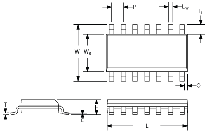
C Clearance between IC body and PCB
H Total carrier height
T Lead thickness
L Total carrier length
LW Lead width
LL Lead length
P Pitch
WB IC body width
WL Lead-to-lead width
O End overhang
Package |
WB |
WL |
H |
C |
L |
P |
LL |
T |
LW |
O |
|---|---|---|---|---|---|---|---|---|---|---|
SOIC-8-N |
3.8–4.0 |
5.8–6.2 |
1.35–1.75 |
0.10–0.25 |
4.8–5.0 |
1.27 |
0.41 (1.04) |
0.19–0.25 |
0.35–0.51 |
0.33 |
SOIC-14-N |
3.8–4.0 |
5.8–6.2 |
1.35–1.75 |
0.10–0.25 |
8.55–8.75 |
1.27 |
1.05 |
0.19–0.25 |
0.39–0.46 |
0.3–0.7 |
SOIC-16-N |
3.8–4.0 |
5.8–6.2 |
1.35–1.75 |
0.10–0.25 |
9.8–10.0 |
1.27 |
1.05 |
0.19–0.25 |
0.39–0.46 |
0.3–0.7 |
SOIC-16-W |
7.4–7.6 |
10.0–10.65 |
2.35–2.65 |
0.10–0.30 |
10.1–10.5 |
1.27 |
0.40–1.27 |
0.20–0.33 |
0.31–0.51 |
0.4–0.9 |
Wide (or extended) SOIC package
Next to the narrow SOIC package (commonly represented as SOx_N or SOICx_N, where x is the number of pins), there's also the wide (or sometimes called extended) version. This package is commonly represented as SOICX_W or SOICx_W.
The difference is mainly related to the parameters WB and WL.
As an example, the values WB and WL are given for an 8-pins wide (extended) SOIC package
Package |
WB |
WL |
|---|---|---|
SOIC-8 |
5.41 (5.16) |
8.07 (7.67) |
Mini- or micro-SOIC package
Another SOIC variant, available only for 8-pins and 10-pins ICs, is the mini-SOIC, also called micro-SOIC. This case is much smaller with a pitch of only 0.5mm. See the following table for the 10-pin model:
Package |
WB |
WL |
H |
C |
L |
P |
LL |
T |
LW |
|---|---|---|---|---|---|---|---|---|---|
miniSOIC-10 |
3.0 |
4.9 |
1.09 |
0.10–0.25 |
3.0 |
0.5 |
0..095 |
0.19 |
0.23 |
SOP
After SOIC came a family of smaller form factors, small outline package (SOP), with a pin spacing of 0.635 mm:
•Plastic small-outline package (PSOP)
•Thin small-outline package (TSOP)
•Thin-shrink small-outline package (TSSOP)
Shrink small-outline package (SSOP) chips have "gull wing" leads protruding from the two long sides, and a lead spacing of 0.025 inches (0.635mm). 0.5mm lead spacing is less common, but not rare.
The body size of a SOP was compressed and the lead pitch tightened to obtain a smaller version SOP. This yields an IC package which is a significant reduction in the size (compared to standard package). All IC assembly processes remain the same as with standard SOPs.
Applications for a SSOP enable end-products (pagers, portable audio/video, disc drives, radio, RF devices/components, telecom) to be reduced in size and weight. Semiconductor families such as operational amplifiers, drivers, optoelectronics, controllers, logic, analog, memory, comparators and more using BiCMOS, CMOS or other silicon / GaAs technologies are well addressed by the SSOP product family.
TSSOP
TSSOPs are particularly suited for gate drivers, controllers, wireless / RF, op-amps, logic, analog, ASICs, memory (EPROM, E2PROM), comparators and optoelectronics. Memory modules, disk drives, recordable optical disks, telephone handsets, speed dialers, video / audio and consumer electronics / appliances are suggested uses for TSSOP packaging.
The ExposedPad variant of small-outline packages can increase heat dissipation by as much as 1.5 times over a standard TSSOP, thereby expanding the margin of operating parameters. Additionally, the ExposedPad can be connected to ground, thereby reducing loop inductance for high frequency applications. The ExposedPad should be soldered directly to the PCB to realize thermal and electrical benefits.
The ICs on DRAM memory modules were usually TSOPs until they were replaced by ball grid array (BGA).