A dual in-line package (DIP or DIL) is an electronic device package with a rectangular housing and two parallel rows of electrical connecting pins. The package may be through-hole mounted to a printed circuit board or inserted in a socket. Dual-in-line packages were developed in the 1960s when the restricted number of leads available on transistor-style packages became a limitation in the use of integrated circuits. Increasingly complex circuits required more signal and power supply leads ( as observed in Rent's rule); eventually microprocessors and similar complex devices required more leads than could be put on a DIP package, leading to development of higher-density packages.
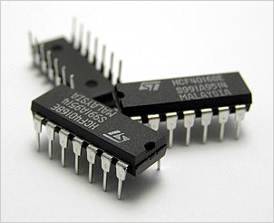
A DIP is usually referred to as a DIPn, where n is the total number of pins. For example, a microcircuit package with two rows of seven vertical leads would be a DIP14. The above photograph shows three DIP14 ICs. Common packages have as few as four and as many as 64 leads. Many analog and digital integrated circuit types are available in DIP packages, as are arrays of transistors, switches, light emitting diodes, and resistors. DIP plugs for ribbon cables can be used with standard IC sockets.
DIP packages are usually made from an opaque molded epoxy plastic pressed around a tin, silver, or gold-plated lead frame that supports the device die and provides connection pins. Some types of IC are made in ceramic DIP packages, where high temperature or high reliability is required, or where the device has an optical window to the interior of the package. Most DIP packages are secured to a printed circuit board by inserting the pins through holes in the board and soldering them in place. Where frequent replacement of the parts is desired, such as in test fixtures or where programmable devices must be removed for changes, a DIP socket is used. Some sockets include a zero insertion force mechanism.
Variations of the DIP package include those with only a single row of pins, possibly including a heat sink tab in place of the second row of pins, and types with four rows of pins, two rows, staggered, on each side of the package. DIP packages have been mostly displaced by surface-mount package types, which avoid the expense of drilling holes in a printed circuit board and which allow higher density of interconnections.
Mounting
DIPs can be mounted either by through-hole soldering or in sockets. Sockets allow easy replacement of a device and eliminate the risk of damage from overheating during soldering. Generally sockets were used for high-value or large ICs, which cost much more than the socket. Where devices would be frequently inserted and removed, such as in test equipment or EPROM programmers, a zero insertion force socket would be used.
DIPs are also used with breadboards, a temporary mounting arrangement for education, design development or device testing. Some hobbyists, for one-off construction or permanent prototyping, use point-to-point wiring with DIPs, and their appearance when physically inverted as part of this method inspires the informal term "dead bug style" for the method.