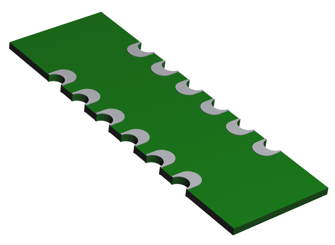
Castellated holes, or castellations, are a special form of semi-plated indentations made along the edges of Printed Circuit Board (PCB) modules. They serve as crucial links to mount one PCB on top of another during the assembly process. These unique holes can take the form of half holes or resemble varying portions of a fragmented circle, depending on the application. They ensure accurate alignment between boards during the soldering process, a procedure known as board-to-board soldering. These features are often found on PCB modules such as Bluetooth or WiFi modules, enabling their use as separate components during the assembly process.

A Castellated PCB
Common methods used in PCB assembly include Through Hole Technology (THT) and Surface Mount Technology. However, when it becomes necessary to stack one PCB over another, board-to-board soldering comes into play. Here, castellations act as connectors between the module and the board it's to be soldered onto.
Why use Castellated holes?
These edge holes are highly beneficial for replicating specific sections of a PCB circuit. For instance, if a circuit includes an inverter, filter, or feedback loops, these sub-circuits can be mass-produced, tested, and when required, soldered onto the main PCB containing other circuit parts.
Applications of Castellated Holes
They serve as breakout boards for certain sections of a larger PCB.
They offer flexibility in changing the Pin layout as per user requirements.
Integrated modules can be mass-produced on a single PCB using castellation, for use in another assembly during production.
PCBs with castellated holes are easily mounted onto another PCB during final production.
They assist in combining two boards to assess the quality of solder joints.
They are ideal for small modules or breakout boards, such as WiFi modules.
They facilitate the creation of wireless PCB to PCB connections.
Designing Castellated Holes
The process of creating castellated holes or vias involves normal via procedures like drilling and copper plating. These holes appear as semi-circles on the board edges because they are cut to form a half hole or partial hole, creating an edge opening. Castellated holes can be formed in several ways.
Recommended Specifications for Castellated Holes
Certain design guidelines should be followed for castellated holes
•Size. Select the largest size possible.
•Surface Finish. This depends on the board's intended application, but electroless nickel immersion gold finish is typically recommended.
•Pad Design. Using the largest possible pad on both top and bottom is recommended.
•Number of Holes. The number of holes depends on the design. It's crucial to find a balance; too many can complicate alignment and assembly.
Use of Castellated holes
Castellated holes on PCBs are widely used across various industries, including telecommunication, computer applications, industrial control, power, automotive, high-end consumer electronics, and more.