The PCB layer stack refers to the arrangement of the layers that make up a printed circuit board. A layer stack is determined by the number and types of layers required for the PCB design.
The layer stack is an essential consideration in PCB design as it affects the electrical performance, manufacturability, and overall functionality of the PCB. Here are some common layer stack configurations for PCBs:
Single-Layer PCB.This is the simplest type of PCB, with components mounted on the top and electrical tracks on the bottom.

A Single-Layer PCB Stack
2-Layer PCB: This is the simplest type of PCB, with a top and bottom layer. 2-layer PCBs are typically used for simple designs with few components and short trace lengths.

A Double-Layer PCB Stack
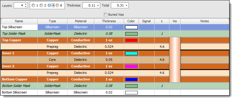
4-Layer PCB: 4-layer PCBs have two signal layers and two ground or power layers. The power or ground planes provide a low impedance path for signals and reduce electromagnetic interference, resulting in improved signal integrity.

A Four-Layer PCB Stack
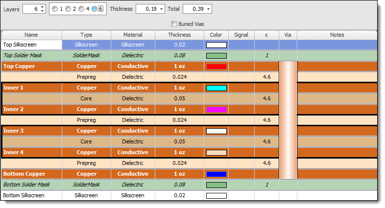
6-Layer PCB: 6-layer PCBs have additional signal layers, providing more flexibility for routing traces and reducing the chances of signal interference.

A Six-Layer PCB Stack
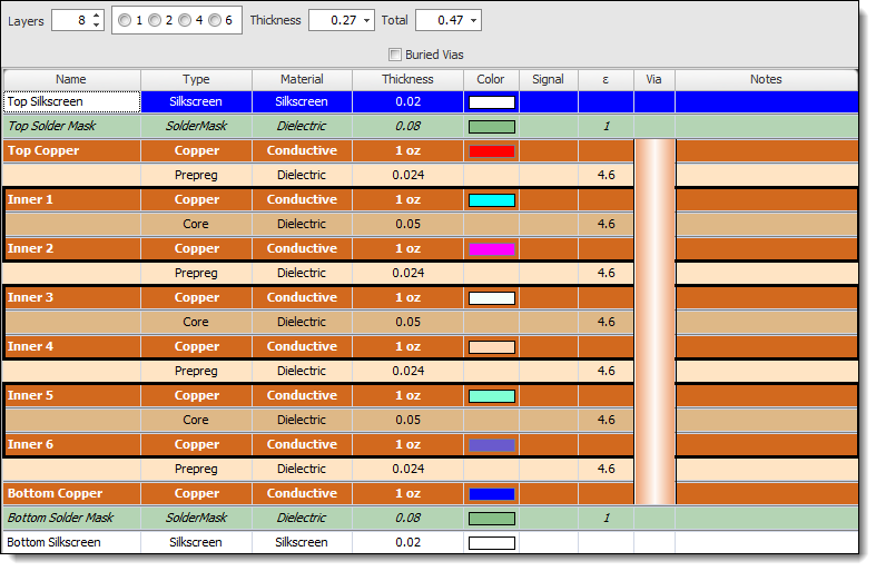
8-Layer PCB: 8-layer PCBs provide even more routing flexibility and can support more complex designs with high-density components and signal requirements.

An Eight-Layer PCB Stack
When designing a layer stack, it is important to consider the following factors:
1.Signal integrity: The layer stack should be designed to minimize the potential for signal interference and ensure the desired signal quality.
2.Power and Ground planes: Adequate power and ground planes should be included in the layer stack to provide low impedance paths for signals, minimize noise, and improve the overall performance of the PCB.
3.Manufacturing constraints: The layer stack should be designed to comply with manufacturing constraints such as the minimum drill size, minimum trace width, and the ability to laminate the layers.
4.Cost: A layer stack with more layers is typically more expensive to manufacture. The design should be optimized to achieve the required electrical performance with the fewest layers possible to reduce the cost of manufacturing.
In summary, the PCB layer stack is a critical aspect of the PCB design process. It affects the electrical performance, manufacturability, and cost of the PCB. Careful consideration should be given to the layer stack design to achieve the desired electrical performance while ensuring manufacturability and keeping costs in check.
A Printed Circuit Layer Stack is a type of layered construction used to construct printed circuit boards (PCBs). The layers are typically made from copper foil, which is then etched and plated with other materials for protection. Typically, each layer has its own purpose and may be used for power supply routing, signal traces, or mounting components. With this type of construction, it is possible to create very complex electrical systems with multiple layers of conductive material in a very small space.
The most common type of stack is the two-layer stackup. As the name suggests, it consists of two layers—the top-side layer and the bottom-side layer—which are separated by a dielectric material such as an epoxy resin. The top-side layer typically consists of a single sheet of copper foil which contains traces that are connected to components on the board. These traces can also be connected to ground plains or other external sources of electricity such as batteries. On the bottom-side layer, there may be additional traces that connect components to each other or to ground plains and external supplies.
In some cases, more than two layers may be used; however, these multi-layer PCBs tend to require more complex manufacturing processes and are not always cost effective for low volume production runs.
When designing and fabricating multiple-layer PCBs, several important considerations must be taken into account including trace spacing between layers, trace widths relative to power supply current requirements, isolation distances between traces and any nearby components or planes in order to avoid interference from stray currents and signals crossing over one another in adjacent layers. Additionally it’s important ensure adequate air gaps between the dielectric material used as insulation between all layers in order prevent short circuits due to capacitive coupling effects between those conductors.
For larger scale designs with multiple types of signals traveling across many different planes within different areas on a board - it’s sometimes necessary to use split planes which separate signals into their respective groups according to their frequency levels in order maintain good signal integrity while minimizing crosstalk issues between various components on the board. In addition - increased trace widths may need to utilized along with additional vias when using high speed signals so that they remain well within acceptable signal tolerances during operation over time without any distortion or loss in quality due transmission line effects arising from adjoining signal lines running parallel together with them on different layers within a stack up configuration.
Finally when making multiple copies of boards using this method - its crucial that each successive design adheres closely enough to the original layout so that assembly process can take place quickly enough without having to make too many changes from duplicate version run batch after batch - thus preserving overall cost effectiveness for large scale fabrication runs where accuracy is paramount for maintaining consistent product specifications throughout every production cycle for years into future if needed!