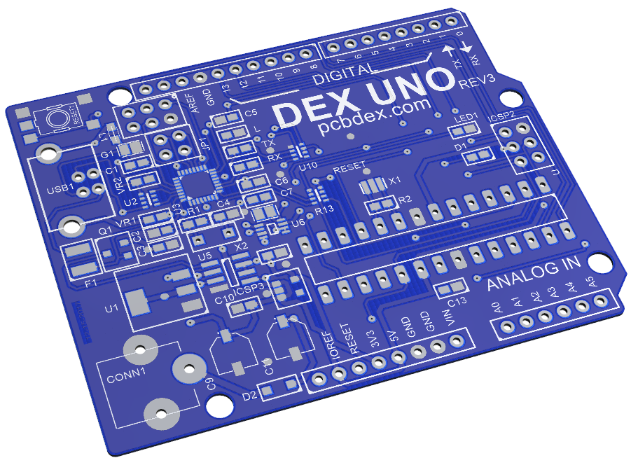
Typical 2-Sided PCB
Designing a printed circuit board (PCB) involves several steps. Here is a general overview of the process:
Measure Twice, Cut Once
"Measure twice, cut once" is a popular adage, particularly in the fields of construction, woodworking, and any craft where precise measurement is crucial. The saying encourages careful preparation and thorough checking to avoid costly or irreversible mistakes.
The underlying principle here is that thorough planning can help prevent mistakes and wasted resources. It's generally easier and less costly to take an extra moment to double-check your work than it is to correct a mistake after it's made. This adage can also be applied metaphorically in various aspects of life where careful planning and consideration are important, such as making financial decisions, planning a project, or making strategic choices.
Define the Specifications
Determine the purpose, functionality, and requirements of your PCB. Consider factors such as the size, number of layers, power requirements, component placement, and signal integrity.

Define the Specifications
Schematic Design
Create a schematic diagram of your circuit using a schematic capture tool. This diagram shows the interconnections between components, helping you visualize the circuit's functionality.
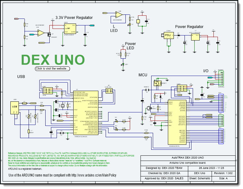
Schematic Design
Component Selection
Choose the components needed for your circuit based on the schematic. Consider factors such as availability, cost, performance, and package size. Ensure that the components you select are suitable for PCB assembly and have appropriate footprints.
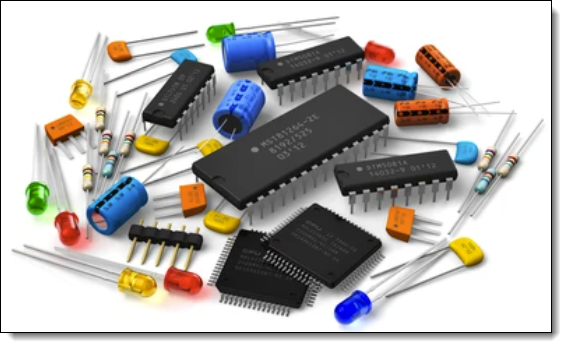
Component Selection
PCB Layout
Transfer the schematic design to a PCB layout tool. Place the components on the PCB, taking into account factors like signal routing, power distribution, and thermal considerations. Arrange the components in a logical and efficient manner, considering the overall size and shape of the PCB.
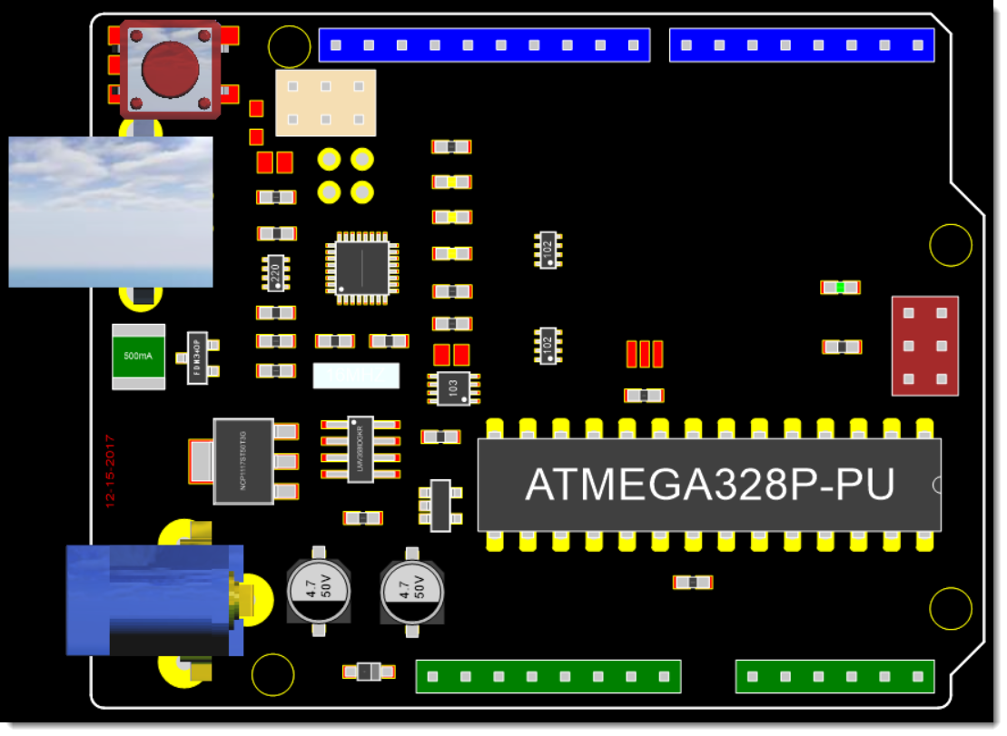
PCB Layout
Routing
Connect the components using copper traces on the PCB. Pay attention to signal integrity, power delivery, and impedance matching. Ensure that the routing is optimized to minimize noise, crosstalk, and other potential issues. Use ground and power planes where necessary to provide stable reference planes.
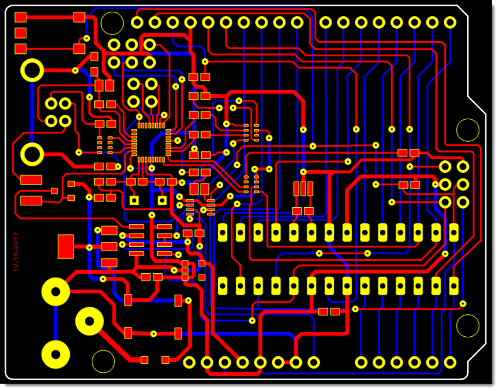
PCB Routing
Design Rule Check (DRC)
Run a design rule check to verify that your PCB layout adheres to the manufacturing constraints, such as minimum trace width, spacing, and clearance requirements. The DRC helps identify potential errors or violations that may impact the functionality or manufacturability of the PCB.
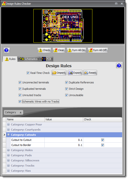
Design Rule Checker
Gerber Files Generation
Once your layout passes the DRC, generate the Gerber files, which are the standard format used by PCB manufacturers to fabricate the board. These files contain all the necessary information about the copper traces, component placement, drill holes, and other features of the PCB.
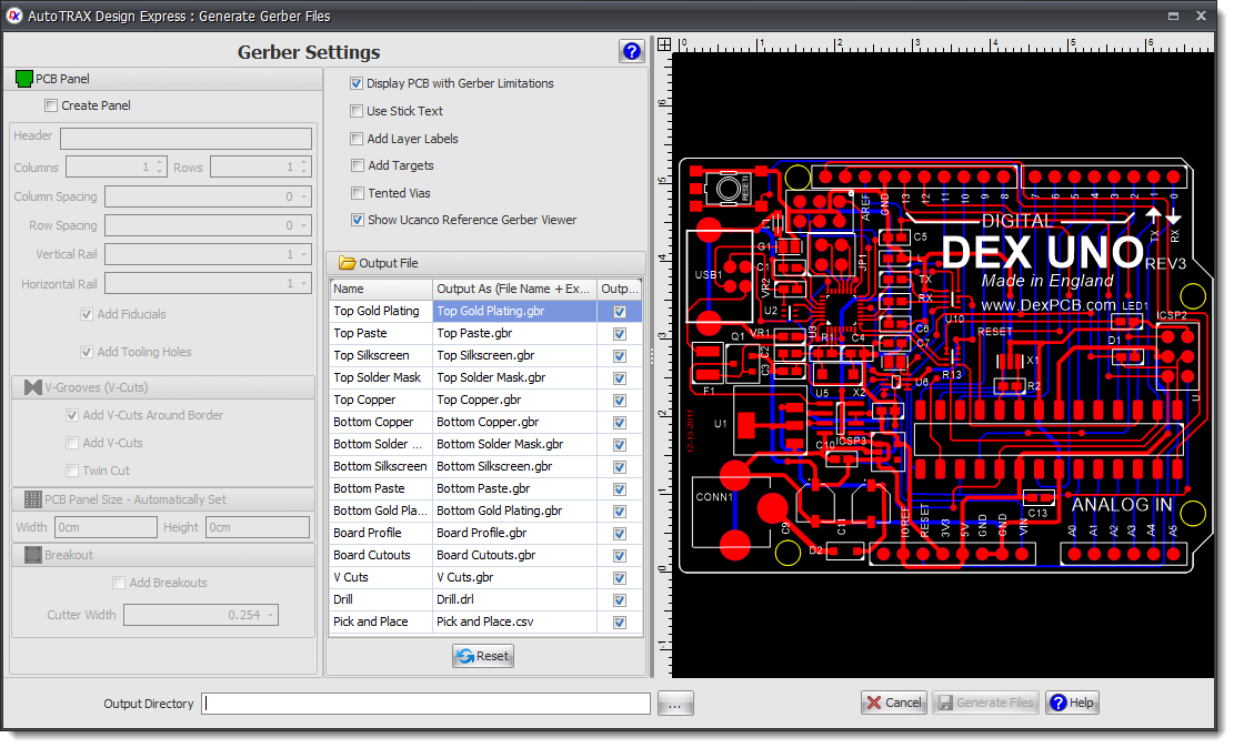
Gerber Files Generation
Prototype and Testing
Order a prototype of your PCB from a manufacturer and assemble it with the chosen components. Test the functionality of the circuit, ensuring that it meets your requirements. If any issues are identified, make necessary revisions to the design.

Prototype and Testing
Manufacturing
Once you are satisfied with the prototype, you can proceed with manufacturing the PCB in larger quantities. Choose a reliable PCB manufacturer who can meet your quality, cost, and time line requirements.
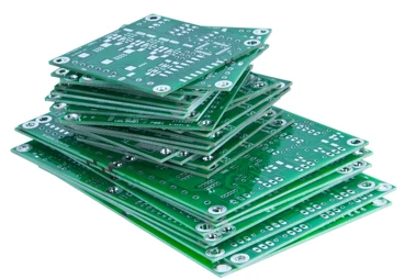
PCB Manufacturing
Assembly and Testing
After receiving the manufactured PCBs, populate them with the required components using either manual or automated assembly methods. Perform thorough testing to ensure the final product functions as intended.
It's important to note that designing a PCB can be complex, and it often requires experience and expertise. Consider consulting with an experienced PCB designer or engineer, especially for more complex projects or if you are new to PCB design. Additionally, there are various PCB design software tools available that can assist you in the design process.
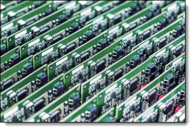
PCB Assembly and Testing