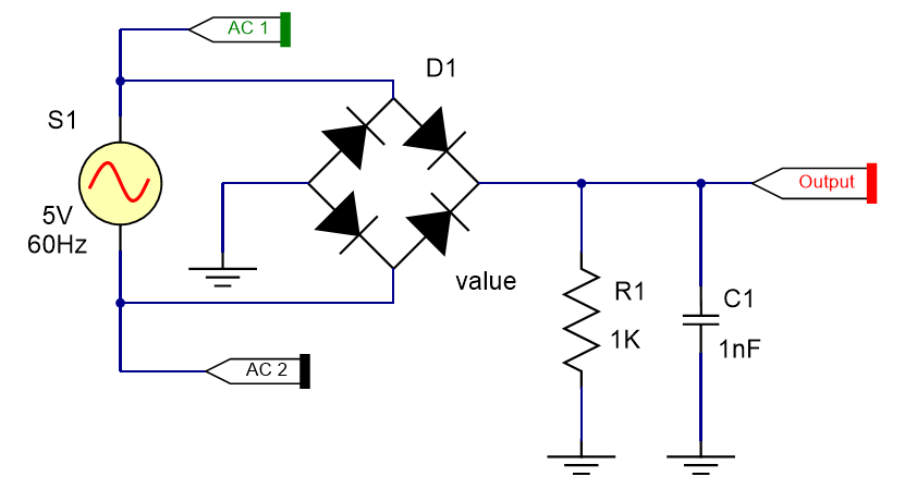
bridge rectifier uses four diodes connected as shown below. When the input cycle is positive as in part (a), diodes D1 and D2 are forward-biased and conduct current in the direction shown. A voltage is developed across R1 that looks like the positive half of the input cycle. During this time, diodes D3 and D4 are reverse-biased.
When the input cycle is negative as in Figure 2–38(b), diodes D3 and D4 are forward biased and conduct current in the same direction through R1 as during the positive half-cycle. During the negative half-cycle, D1 and D2 are reverse-biased. A full-wave rectified output voltage appears across R1 as a result of this action.
Bridge Output Voltage
A bridge rectifier with a transformer-coupled input is shown in Figure 2–39(a). During the positive half-cycle of the total secondary voltage, diodes D1 and D2 are forward-biased. Neglecting the diode drops, the secondary voltage appears across the load resistor. The same is true when D3 and D4 are forward-biased during the negative half-cycle.
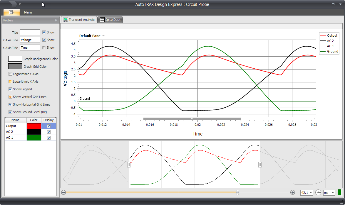
The Spice Probe shows the electrical signals.